
Sometimes you need to control multiple devices such as LEDs, sensors, or modules with your Arduino. As the number of peripheral devices increases, you will quickly run out of GPIO pins of Arduino. How would you expand your Arduino’s capabilities? The answer is to use a shift register that can effectively increase the number of output/input pins available to the Arduino.
There are two types of shift register: SIPO (Serial In Parallel Out) and PISO (Parallel in Serial Out). SIPO registers like 74HC595 IC’s are used to increase the number of outputs. PISO registers like 74HC165 IC’s are used to increase the number of inputs.
This article focuses on one of the most widely used SIPO shift register ICs- 74HC595. It allows you to interface 8 devices using only 3 pins of Arduino. What’s even better? You can daisy-chain multiple shift registers together to interface a large number of peripherals.
Whether you’re lighting up an LED array, creating a multiplexed display, or building a project that requires serial communication for outputs, 74HC595 is the ideal choice. In this tutorial, we’ll explore the working of the 74HC595 shift register and interface it with an Arduino. Let’s get started!
What is a Shift Register and Why Use It?
The 74HC595 is an 8-bit serial-in-parallel-out shift register IC with D-type latch. It has 3 output states: HIGH, LOW, or HIGH-Impedance (disconnected). The outputs can be put in a HIGH-Impedance state, allowing multiple devices to share the same output lines.
Let’s take an example to understand where you can use it. Suppose you want to create a light animation or patterns on an 8×8 LED matrix, which has 64 LEDs. Each LED in the matrix requires a dedicated control line. Controlling all 64 LEDs individually would need 64 pins, which is not possible with a typical microcontroller like an Arduino Uno which only has 14 digital I/O pins. In this case using two shift registers one for rows and another for columns, you can control the entire LED matrix with just 6 pins from the microcontroller.
It’s important to note that shift registers provide only digital outputs, meaning they can only switch devices ON or OFF (logic HIGH or logic LOW). They cannot handle analog operations like dimming LEDs but there are some ways using them we can control the brightness of LEDs connected to output.
Features of the 74HC595
- 8-bit parallel output
- Serial-to-parallel data conversion
- Cascading capability for expanding outputs
- Low power consumption
- Compatible with 5V logic levels
- Supply voltage of 2.0 to 6.0
How does the 74HC595 Shift Register Work?
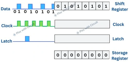
74HC595 shift register IC contains two registers: shift register and storage register (latch).
The data is entered into the shift register one bit at a time. Each time a clock pulse is sent to the shift register clock (SRCLK) pin, the data bits in the shift register move one position to the left (From LSB to MSB) inside the Shift Register. Consecutively, the LSB of the shift register takes the current state of the DATA pin (either HIGH or LOW). This process continues until all 8 bits are loaded into the shift register.
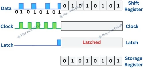
Once all 8 bits are loaded into the shift register, the LATCH pin is enabled and data from the shift register is copied to the storage register. The storage register drives the output pins (QA to QH), thus any changes in the storage register directly update the output states.
If multiple 74HC595 ICs are cascaded, the most significant bit (MSB) of the shift register is passed to the next IC via the Cascade Output (QH‘). This enables seamless chaining of multiple ICs for expanding output control.
74HC595 Pinout
The pin configuration of the 74HC595 shift register is shown below.
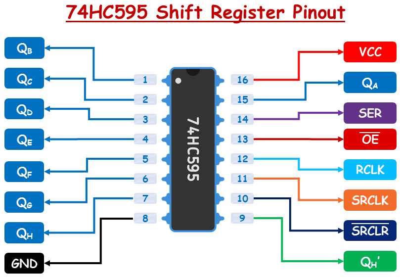
Outputs (QA to QH) The 74HC595 has eight output pins labelled QA to QH (sometimes referred to as Q0 to Q7. These pins represent the eight bits of data stored in the storage register. Each output corresponds to one bit of the stored data. On IC output QA, QB, QC, QD, QE, QF, QG, QH pins are pin 13, 1, 2, 3, 4, 5, 6, 7 respectively.
Serial Data Input (SER) This pin is used to provide data bit by bit into the shift register.
Shift Register Clock (SRCLK) This clock pin is used to shift data into the shift register. Each rising (LOW to HIGH) edge of the clock signal moves the data one position along the shift register(from LSB to MSB), making room for the next bit of data. The timing of this signal is critical for correctly loading data into the register.
Storage Register Clock/Latch (RCLK) This pin plays a critical role in how a shift register operates. When the RCLK pin goes from LOW to HIGH, the data currently held in the shift register is copied into the storage register. The data transferred to the storage register is then sent to the output pins (QA-QH).
Cascade Output (QH‘) The cascade output allows multiple 74HC595 ICs to be connected in series to control a larger number of outputs. The QH‘ pin outputs the value of the last bit (bit 7) from the shift register. If this pin is connected to the SER input pin of another 74HC595 shift register and the same clock signal is fed to both ICs, outputs are increased to 16.
Output Enable (OE) This pin enables or disables all outputs simultaneously. It is an active LOW pin, meaning the outputs are enabled when this pin is pulled LOW. When pulled HIGH, all outputs go into a high-impedance state (essentially disconnecting them), which is useful in applications where multiple devices share the same data lines. By applying a PWM signal at this pin we can control the brightness of LEDs connected at outputs.
Shift Register Clear (SRCLR) This pin clears all the data in the shift register when pulled LOW. It is an active LOW pin and resets the shift register to zero. Clearing the shift register does not affect the storage register. Normally this pin is connected to Vcc.
VCC The VCC pin is the power supply pin and it is connected to 5V.
GND This is the ground pin.
Functional Description of 74HC595 IC
Here is the function table which describes the various functional modes of 74HC595 IC.
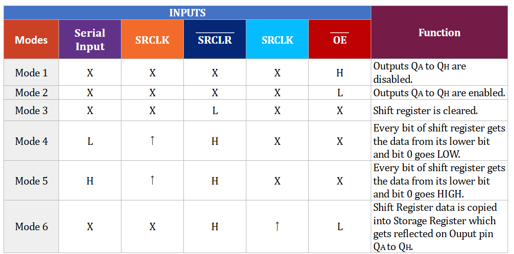
Here,
X -> represents don’t care, whether pin is in HIGH or low state it doesn’t matter
| -> this indicates the pin is in LOW to HIGH transition.
L -> pin is LOW
H -> pin is HIGH
Mode 1 When the Output Enable pin (which is Active LOW) is HIGH all outputs (QA to QH) are disabled i.e., all output pins go into the HIGH impedance state regardless of the states of all other input pins hence, they don’t care.
Mode 2 When the Output Enable pin is LOW all outputs (QA to QH) are enabled, the states of all other input pins don’t matter hence, they don’t care.
Mode 3 When the Shift Register Clear (SRCLR) pin (which is Active LOW) is LOW, the shift register resets to zero, regardless of the clock or state of the other pins.
Mode 4 When the Shift Register Clock (SRCLK) goes LOW to HIGH, and Serial Input (SER) pin is LOW then all bits in the shift register are shifted to Left and its bit 0 goes LOW. Make sure the shift register clear pin is HIGH.
Mode 5 When the Shift Register Clock goes LOW to HIGH and the Serial Input pin is HIGH then all the bits in the shift register are shifted to left and its bit 0 goes HIGH. Make sure the Shift Register Clear pin is HIGH.
Mode 6 When the Latch Pin or Storage Register Clock pin goes from LOW to HIGH then all the data which is present in shift register gets copied into storage register and hence it is reflected on the output pins QA to QH. Make sure the Shift Register Clear pin is HIGH and Output Enable pin is LOW. The states of other input pins don’t matter.
Wiring a 74HC595 Shift Register to an Arduino
Now that we’ve covered the working and functional modes of the 74HC595 shift register, let’s start interfacing it with an Arduino UNO. We will be controlling all 8 outputs of the shift register using three pins of Arduino. We will also control the brightness of the LED using the PWM pin of Arduino.
Hardware Requirement
| Component Name | Quantity | Remarks | Where to Buy |
|---|---|---|---|
| Arduino Uno R3 | 1 | Revision R3 | Amazon.com |
| 74HC595 shift register | 1 | 8-bit SIPO shift register IC | Amazon.com |
| 8 LEDs | 8 | To show output | Amazon.com |
| Resistor 220Ω | 8 | Required for LEDs | Amazon.com |
| Connecting wires | Multiple | For connecting shift register with Arduino | Amazon.com |
| Breadboard | 1 | Full Size | Amazon.com |
| USB cable type A/B | 1 | for programming Arduino UNO | Amazon.com |
Software Requirement
Arduino IDE, Version 2.3.4 or above installed on your PC
Wiring Diagram
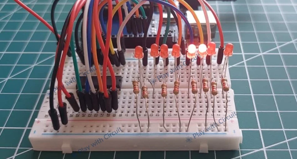
Here, we will be controlling 8 red LED’s using 74HC595 IC which are connected at output QA to QH.
Start by placing the 74HC595 IC on the breadboard. Ensure each side of IC pins goes into different halves of the breadboard.
Now to find Pin 1, check for the small notch or dot on the IC — Pin 1 is present to the left of the notch.
Next let’s supply the power to the shift register. Connect Pin 16 (VCC) and pin 10 (SRCLR) to the 5V output from the Arduino. Now connect pin 8 (GND) to GND on the Arduino. Connect pin 13 (OE) to pin 9 of Arduino.
Now let’s connect the three control pins. The shift register is controlled by three pins from the Arduino. Connect pin 11 (SRCLK) of the shift register to pin 12 on the Arduino, which acts as the clock input for shifting data. Then, connect pin 12 (RCLK) to pin 10 of Arduino, which latches the data to the output pins. Next, connect pin 14 (SER), the serial data input pin, to pin 11 of the Arduino.
Then connect the anodes of the 8 LEDs to output pins QA to QH of the shift register. Also, connect 220Ω resistor in series with each LED. This prevents the LEDs from drawing too much current and damaging them. The cathode of each LED is connected to the Ground pin of Arduino via 220 ohm resistance.
The following diagram shows how to wire everything together:

Here are the connections between 74HC595 shift register and Arduino:
| 74HC595 Side Pin | Connected to |
|---|---|
| Pin 1 – QB | Anode of LED |
| Pin 2 – QC | Anode of LED |
| Pin 3 – QD | Anode of LED |
| Pin 4 – QE | Anode of LED |
| Pin 5 – QF | Anode of LED |
| Pin 6 – QG | Anode of LED |
| Pin 7 – QH | Anode of LED |
| Pin 8 – GND | GND pin of Arduino |
| Pin 9 – QH’ | Not connected |
| Pin10 - SRCLR | Connected to 5V pin of Arduino |
| Pin11 - SRCLK | Pin 12 of Arduino |
| Pin12 – RCLK/Latch | Pin 10 of Arduino |
| Pin13 – OE | Pin 9 of Arduino |
| Pin14 – SER | Pin 11 of Arduino |
| Pin15 - QA | Anode of LED |
| Pin 16 - VCC | Connected to 5V pin of Arduino |
Arduino Code for Interfacing 74HC595 Shift Register with Arduino
In the below code we will be using inbuilt library functions of the Arduino IDE to light up the LED using the shift register IC. OE pin of the shift register IC is used to control the brightness of the LED.
Upload the following code to Arduino and observe how the LEDs sequentially turn ON and OFF with varying brightness.
/*
Code to interface 74HC595 SIPO shift register using Arduino UNO
by www.playwithcircuit.com
*/
//Pin connected to SH_CP of 74HC595
int clockPin = 12;
//Pin connected to DS of 74HC595
int dataPin = 11;
//Pin connected to ST_CP of 74HC595
int latchPin = 10;
//Pin connected to OE of 74HC595
int brightnessPin = 9;
//Brightness control variable
int PWM_Value = 0;
void setup() {
  //set pins to output so you can control the shift register  and initially they should be HIGH
  pinMode(latchPin, OUTPUT);
  pinMode(clockPin, OUTPUT);
  pinMode(dataPin, OUTPUT);
  pinMode(brightnessPin, OUTPUT);
  digitalWrite(latchPin, HIGH);
  digitalWrite(clockPin, HIGH);
  digitalWrite(dataPin, HIGH);
  analogWrite(brightnessPin, 255);
}


void loop() {
  int led_byte = 0x00;
  //  turn ON all LEDs one by one
  for (int i = 0; i < 8; i++) {
    // adjust the brightness of LEDs
    PWM_Value = (255 - (115 + (20*i)));
    analogWrite(brightnessPin, PWM_Value);
    led_byte |= (0x01 << i);
    // take the latchPin low
    digitalWrite(latchPin, LOW);
    // shift out the bits:
    shiftOut(dataPin, clockPin, MSBFIRST, led_byte);
    //take the latch pin high so the LEDs will light up:
    digitalWrite(latchPin, HIGH);
    // pause before next value:
    delay(100);
  }
  //  turn OFF all LEDs one by one
  for (int i = 0; i < 8; i++) {
    led_byte &= ~(0x01 << i);
    // make the latchPin low
    digitalWrite(latchPin, LOW);
    // shift out the bits:
    shiftOut(dataPin, clockPin, MSBFIRST, led_byte);
    //make the latch pin high so the LEDs will light up:
    digitalWrite(latchPin, HIGH);
    // pause before next value
    delay(100);
  }
}
Code Description
Firstly we define four control pins: clock, data, latch and brightness that control the 74HC595 shift register and the brightness of the LEDs. These pins are connected to pins 12, 11, 10, and 9 on the Arduino.
//Pin connected to SH_CP of 74HC595
int clockPin = 12;
//Pin connected to DS of 74HC595
int dataPin = 11;
//Pin connected to ST_CP of 74HC595
int latchPin = 10;
//Pin connected to OE of 74HC595
int brightnessPin = 9;
We also define a variable PWM_Value that we’ll use to control the brightness level of the LEDs using Pulse Width Modulation.
//Brightness control variable
int PWM_Value = 0;
In the setup() function, we configure all the four control pins as outputs so that the Arduino can communicate with the shift register and adjust the LED brightness. The control pins—latchPin, clockPin, and dataPin—are initially set to HIGH. This ensures that the LEDs are in a known state when the program starts. The brightnessPin is initially set to full brightness (255).
void setup() {
  //set pins to output so you can control the shift register  and initially they should be HIGH
  pinMode(latchPin, OUTPUT);
  pinMode(clockPin, OUTPUT);
  pinMode(dataPin, OUTPUT);
  pinMode(brightnessPin, OUTPUT);
  digitalWrite(latchPin, HIGH);
  digitalWrite(clockPin, HIGH);
  digitalWrite(dataPin, HIGH);
  analogWrite(brightnessPin, 255);
}
Now in the loop() function, we first declare a variable called led_byte and initialize it to 0x00, which means all 8 bits (and thus all 8 LEDs) are initially OFF.
for loop is used to turn ON all LEDs one by one. The loop runs 8 times—once for each LED connected to the shift register.
Inside the loop, we gradually increase the brightness of each subsequent LED. The brightness is controlled by calculating a PWM_Value which increases for each LED turned ON.
Then, we use bitwise OR (|=) to set a specific bit in the led_byte variable, turning ON the corresponding LED.
Before shifting out the new led_byte value to the shift register, we bring the latchPin LOW to temporarily hold the output. We then send the updated byte to the shift register using shiftOut(), and set the latch pin HIGH again to display the result on the LEDs.
After an LED is turned ON, we pause for 100 ms then light the next one.
  //  turn ON all LEDs one by one
  for (int i = 0; i < 8; i++) {
    // adjust the brightness of LEDs
    PWM_Value = (255 - (115 + (20*i)));
    analogWrite(brightnessPin, PWM_Value);
    led_byte |= (0x01 << i);
    // make the latchPin low
    digitalWrite(latchPin, LOW);
    // shift out the bits
    shiftOut(dataPin, clockPin, MSBFIRST, led_byte);
    //make the latch pin high so the LEDs will light up
    digitalWrite(latchPin, HIGH);
    // pause before next value
    delay(100);
  }
Once all LEDs are ON, another for loop is used to turn them OFF, one by one. This time, we use bitwise AND with a bitwise NOT to clear (turn OFF) individual bits in led_byte.
We follow the same shifting and latching process as above to update the shift register and turn OFF LEDs.
  //  turn OFF all LEDs one by one
  for (int i = 0; i < 8; i++) {
    led_byte &= ~(0x01 << i);
    // make the latchPin low
    digitalWrite(latchPin, LOW);
    // shift out the bits
    shiftOut(dataPin, clockPin, MSBFIRST, led_byte);
    //make the latch pin high so the LEDs will light up
    digitalWrite(latchPin, HIGH);
    // pause before next value
    delay(100);
  }
}
Arduino Code using Bit-banging Technique to Control 74HC595 Shift Register IC
The functionality of below code is the same as above code but here we didn’t use any inbuilt library function.
/*
Code to Interface 74HC595 SIPO shift register Using Arduino UNO
by www.playwithcircuit.com
Bit Banging code is used
*/

#define CLOCK 12
#define DATA 11
#define LATCH 10
#define PWM 9

#define CLOCK_HIGH digitalWrite(CLOCK, HIGH);
#define CLOCK_LOW digitalWrite(CLOCK, LOW);

#define DATA_HIGH digitalWrite(DATA, HIGH);
#define DATA_LOW digitalWrite(DATA, LOW);

#define LATCH_HIGH digitalWrite(LATCH, HIGH);
#define LATCH_LOW digitalWrite(LATCH, LOW);

#define CLOCK_PULSE \
  { CLOCK_LOW DELAY CLOCK_HIGH }  // this is used as clock pulse for row IC

#define LATCH_PULSE \
  { LATCH_LOW DELAY LATCH_HIGH }  // this is used as latch pulse for row IC

#define DELAY delayMicroseconds(1);

//Brightness control variable
int PWM_Value = 0;

void setup() {
  //set pins to output so you can control the shift register and initially they should be HIGH
  pinMode(CLOCK, OUTPUT);
  pinMode(DATA, OUTPUT);
  pinMode(LATCH, OUTPUT);
  pinMode(PWM, OUTPUT);

  digitalWrite(CLOCK, HIGH);
  digitalWrite(DATA, HIGH);
  digitalWrite(LATCH, HIGH);
  analogWrite(PWM, 255);
}
void loop() {
  //  turn ON all LEDs one by one
  DATA_HIGH  // Put Data High on Serial Input Pin
  for (int i = 0; i < 8; i++) {
    // adjust the brightness of LEDs
    PWM_Value = (255 - (115 + (20*i)));
    analogWrite(PWM, PWM_Value);
    CLOCK_PULSE
    LATCH_PULSE  // Provide Low to High Pulse on Latch Pin to Latch the data on the pins
    delay(100);
  }
  //  turn OFF all LEDs one by one
  DATA_LOW  // Put Data Low on Serial Input Pin
  for (int i = 0; i < 8; i++) {
    CLOCK_PULSE
    LATCH_PULSE  // Provide Low to High Pulse on Latch Pin to Latch the data on the pins
    delay(100);
  }
}
Code Description
At the beginning of the code, we define four pins on the Arduino that are used to control the 74HC595 shift register:
#define CLOCK 12
#define DATA 11
#define LATCH 10
#define PWM 9
Next, we define several macros. These macros represent digital HIGH/LOW states and pulses.
Two special macros, CLOCK_PULSE and LATCH_PULSE, combine LOW-HIGH transitions with a microsecond delay in between, which simulate the rising-edge pulses required by the shift register to shift data or update outputs. The DELAY macro adds a tiny delay between transitions to ensure stable signal timing, which is especially important in bit-banging techniques.
Then we declare a variable named PWM_Value.
#define CLOCK_HIGH digitalWrite(CLOCK, HIGH);
#define CLOCK_LOW digitalWrite(CLOCK, LOW);

#define DATA_HIGH digitalWrite(DATA, HIGH);
#define DATA_LOW digitalWrite(DATA, LOW);

#define LATCH_HIGH digitalWrite(LATCH, HIGH);
#define LATCH_LOW digitalWrite(LATCH, LOW);

#define CLOCK_PULSE \
  { CLOCK_LOW DELAY CLOCK_HIGH }  // this is used as clock pulse for row IC

#define LATCH_PULSE \
  { LATCH_LOW DELAY LATCH_HIGH }  // this is used as latch pulse for row IC

#define DELAY delayMicroseconds(1);

//Brightness control variable
int PWM_Value = 0;
In the setup() function, we configure all control pins as outputs using pinMode(). Then initialize all control pins (CLOCK, DATA, LATCH) to a HIGH state. Then we set the PWM pin to full brightness 255.
void setup() {
  //set pins to output so you can control the shift register and initially they should be HIGH
  pinMode(CLOCK, OUTPUT);
  pinMode(DATA, OUTPUT);
  pinMode(LATCH, OUTPUT);
  pinMode(PWM, OUTPUT);

  digitalWrite(CLOCK, HIGH);
  digitalWrite(DATA, HIGH);
  digitalWrite(LATCH, HIGH);
  analogWrite(PWM, 255);
}
In the loop() function, first we set the DATA pin HIGH using the DATA_HIGH macro.
A for loop runs from 0 to 7, iterating once for each of the 8 bits (or LEDs). In each iteration, the PWM value is calculated. The calculated PWM_Value is then applied to the PWM pin using analogWrite function.
After that, a CLOCK_PULSE shifts the HIGH bit into the shift register, and a LATCH_PULSE updates the outputs so the corresponding LED lights up.
void loop() {
  //  turn ON all LEDs one by one
  DATA_HIGH  // Put Data High on Serial Input Pin
  for (int i = 0; i < 8; i++) {
    // adjust the brightness of LEDs
    PWM_Value = (255 - (115 + (20*i)));
    analogWrite(PWM, PWM_Value);
    CLOCK_PULSE
    LATCH_PULSE  // Provide Low to High Pulse on Latch Pin to Latch the data on the pins
    delay(100);
  }
After turning on all 8 LEDs, the next loop turns them off one by one. First, the DATA pin is set LOW using the DATA_LOW macro. This means the register will now receive a series of logical ‘0’ bits with each pulse.
In for loop, CLOCK_PULSE shifts the LOW bit into the register. LATCH_PULSE updates the output pins after each shift.
  //  turn OFF all LEDs one by one
  DATA_LOW  // Put Data Low on Serial Input Pin
  for (int i = 0; i < 8; i++) {
    CLOCK_PULSE
    LATCH_PULSE  // Provide Low to High Pulse on Latch Pin to Latch the data on the pins
    delay(100);
  }
}
Cascading Multiple 74HC595 ICs
Cascading the 74HC595 IC is required to increase the number of output pins which can be controlled by Arduino. The most common form of cascading the shift register IC is the Daisy Chain Configuration.
In this configuration the QH’ pin of the first IC is connected to the SER pin of the second IC. The QH’ pin of the second IC is connected to the SER pin of the third IC. The SRCLK, OE, SRCLR, RCLK are connected parallelly with the controller.
The advantages of this type of connection is that all the cascaded IC’s can be controlled with the same pin of the controller. The disadvantage is that as the number of cascaded IC increases there is delay in controlling the output.
Wiring Multiple 74HC595 Shift Registers to an Arduino
Here, we will connect three 74HC595 shift register ICs, connected in Daisy Chain Configuration with an Arduino UNO. We will be controlling all 24 outputs of three shift registers using three pins of Arduino.
Hardware Requirement
| Component Name | Quantity | Remarks | Where to Buy |
|---|---|---|---|
| Arduino Uno R3 | 1 | Revision R3 | Amazon.com / Amazon.in |
| 74HC595 shift register | 3 | 8-bit SIPO shift register IC | Amazon.com / Amazon.in |
| LEDs | 24 | For Output | Amazon.com / Amazon.in |
| Resistor 220Ω | 24 | For LEDs | Amazon.com / Amazon.in |
| Connecting wires | Multiple | For connecting shift register with Arduino | Amazon.com / Amazon.in |
| Breadboard | 3 | Full Size | Amazon.com / Amazon.in |
Software Requirement
Arduino IDE, version 2.3.4 or above installed on your PC
Wiring Diagram
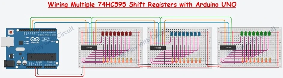
The wiring remains the same between Arduino and 74HC595 IC. SRCLK, RCLK/Latch pins of all the shift register IC are parallelly connected to pin 12 and pin 10 of Arduino UNO.
Pin 11 of Arduino is connected to SER pin of first shift register, QH’ of first shift register is connected to SER pin of second shift register and QH’ of second shift register is connected to SER pin of third shift Register.
Since this time, we are not controlling the brightness of LEDs hence, the OE pins of all the ICs are connected to GND. The SRCLR pin of all ICs is connected to VCC. Power and GND pins of all the ICs are connected to 5V and GND pin Arduino.
Arduino Code for interfacing Multiple 74HC595 Shift Registers to an Arduino
/*
Code to interface three 74HC595 SIPO shift register using Arduino UNO
by www.playwithcircuit.com
Bit Banging Code is Used
*/

#define CLOCK 12
#define DATA 11
#define LATCH 10

#define CLOCK_HIGH digitalWrite(CLOCK, HIGH);
#define CLOCK_LOW digitalWrite(CLOCK, LOW);

#define DATA_HIGH digitalWrite(DATA, HIGH);
#define DATA_LOW digitalWrite(DATA, LOW);

#define LATCH_HIGH digitalWrite(LATCH, HIGH);
#define LATCH_LOW digitalWrite(LATCH, LOW);

#define CLOCK_PULSE \
  { CLOCK_LOW DELAY CLOCK_HIGH }  // this is used as clock pulse for row IC

#define LATCH_PULSE \
  { LATCH_LOW DELAY LATCH_HIGH }  // this is used as latch pulse for row IC

#define DELAY delayMicroseconds(1);

void setup() {
  //set pins to output so you can control the shift register and initially they should be HIGH
  pinMode(CLOCK, OUTPUT);
  pinMode(DATA, OUTPUT);
  pinMode(LATCH, OUTPUT);
  digitalWrite(CLOCK, HIGH);
  digitalWrite(DATA, HIGH);
  digitalWrite(LATCH, HIGH);
}
void loop() {
  //  turn ON all LEDs one by one
  DATA_HIGH         // Put Data High on Serial Input Pin
  SendData();       // Push data into the Shift Registers
  //  turn OFF all LEDs one by one
  DATA_LOW          // Put Data Low on Serial Input Pin
  SendData();       // Push data into the Shift Registers
}

void SendData() {    // Push data into the Shift Registers
  for (int i = 0; i < 24; i++)
{
    CLOCK_PULSE
    LATCH_PULSE  // Provide Low to High Pulse on Latch Pin to Latch the data on the pins
    delay(100);
  }
}
Code Description
Here we define pins and macros like previous code.
In the loop() function, first we set the data line to HIGH. This means all bits shifted into the shift registers will be 1, turning all LEDs ON one by one.
Then we call SendData() function to shift HIGH bits in. Next, we set the data line to LOW, meaning all bits will be 0. Again, we call SendData() to shift LOW bits in, which turns LEDs OFF one by one.
SendData() function does the bit shifting into the 74HC595 registers. It runs a loop 24 times because we are using 3 shift registers × 8 bits = 24 outputs.
Inside each loop iteration, CLOCK_PULSE causes the data (HIGH or LOW) currently on the DATA pin to be shifted into the first 74HC595. LATCH_PULSE immediately updates the outputs of all 3 shift registers with the new data.


