
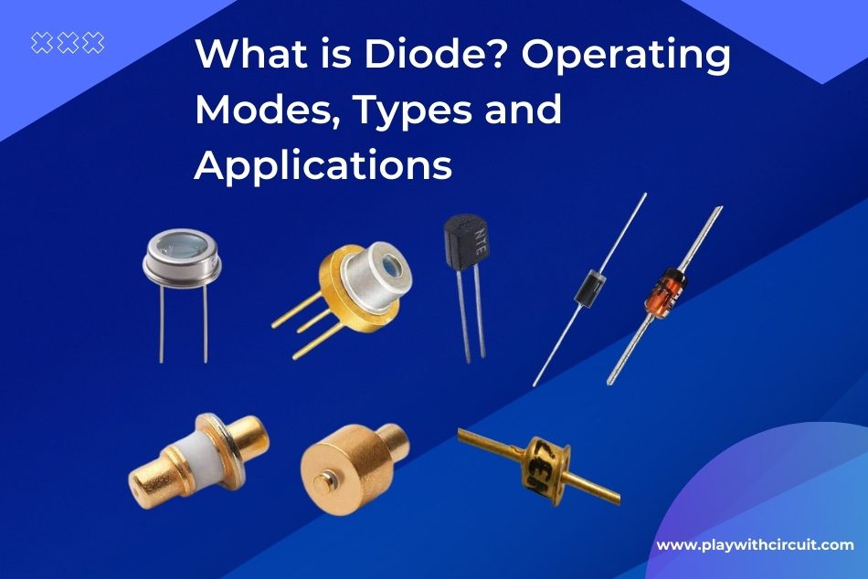
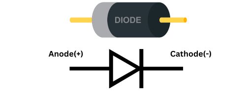
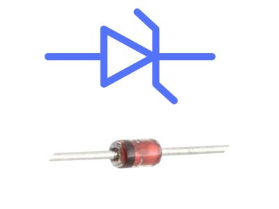
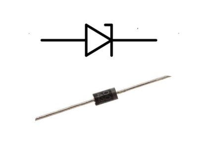
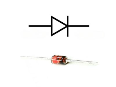
A diode is a two-terminal electronic component that allows current to flow in one direction. It is one of the most widely used semiconductor components in modern-day electronics.
In this article, we will learn about diodes, their working, types and applications.
What is a Diode?
A diode is an important component in a circuit that performs many critical functions such as transforming alternating current to direct current and protecting circuits by limiting the voltage. They can also be used as signal limiters, switches, signal modulators, signal mixers, etc.
An ideal diode has zero resistance in one direction, and infinite resistance in the reverse direction. But practically, diodes have negligible resistance in one direction (to allow current flow), and very high resistance in the reverse direction (to prevent current flow).
Most of the diodes are created by using semiconductors materials like silicon and germanium. A diode consists of two layers n-type and p-type semiconductor material. N-type semiconductor is created by doping an intrinsic semiconductor with pentavalent or donor impurity such as antimony. P-type semiconductor is created by doping an intrinsic semiconductor with trivalent or acceptor impurity such as boron.
If we dope a piece of silicon such that part of it is n-type and the other part is p-type, a boundary called pn junction is formed between the two regions and A basic diode is created.
Diode Operation
In the N region, the majority of charge carriers are electrons and the minority of charge carriers are holes. In the P region, the majority of charge carriers are holes and the minority of charge carriers are electrons. In the n region, free electrons are randomly drifting in all directions.
At the instant of pn junction formation, free electrons in the n region near the junction start diffusing across the junction into the p region where they combine with holes near the junction.
So, the n region loses free electrons which creates a layer of positive charges near the junction. As electrons and holes combine, the p region loses holes which creates a layer of negative charges near the junction. These two layers of positive and negative charges form the depletion region. This depletion region is formed very quickly and is very thin compared to the two n and p regions.
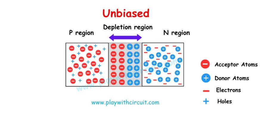
After the initial diffusion of free electrons into the p region, a point is reached where negative charges in the depletion region repel further diffusion of electrons across the junction so diffusion stops. So the depletion region acts as a barrier that prevents any further diffusion of charge carriers across the junction.
Barrier Potential: In the depletion region there are positive and negative charges on opposite sides of pn junction so there is a force acting on charges called an electric field. This electric field is a barrier to movement of electrons and external energy source is required to get the electrons to move across this barrier.
The barrier potential is the potential difference of the electric field across the junction which is the amount of voltage required to move electrons through the depletion region.
Biasing the pn Junction Diode
Since no electrons flow through the pn junction at equilibrium. So we use an external voltage to bias the diode. We connect a dc voltage source in proper polarity with the diode so it allows the flow of majority carriers and conducts electric current. There are two bias conditions: forward and reverse.
Forward Bias
In forward-bias condition, we connect a voltage source (battery) with the diode in such a way that the positive terminal of the battery is connected to the p region and the negative terminal is connected to the n region of the diode. This bias condition allows current through the diode.
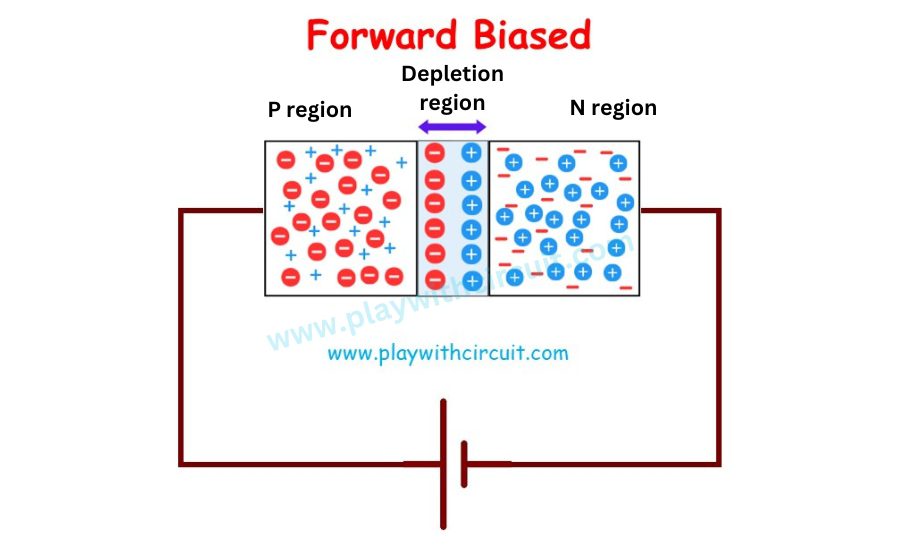
The external bias voltage should be more than the barrier potential which is 0.7 volt for silicon diodes and 0.3 volt for germanium diodes. When the external voltage applied across the diode becomes more than the forward barrier potential, the free majority charge carriers start crossing the barrier and forward diode current starts flowing.
Now let us see what happens in forward-bias. As shown in figure, the negative terminal of the battery pushes the free electrons (majority carriers) in n region towards the junction. The bias voltage provides sufficient energy to electrons to cross the barrier potential of depletion region and move to p region. Now in the p region, holes provide the pathway to move these electrons through the p region. The electron moves from one hole to another hole to the left and the positive terminal of the battery attracts these electrons. This movement of free electrons is called electric current.
Reverse Bias
In reverse bias condition, we connect a battery with the diode in such a way that the positive terminal of a battery is connected to the n-type side and the negative terminal is connected to the p-type side of the diode. This state basically prevents current through the diode.
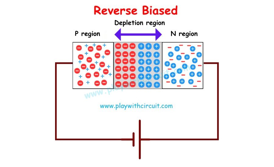
Now let us see what happens in reverse-bias. As shown in figure, in this state, the holes in the p region and electrons in the n region are pulled away from the junction. This causes the creation of more positive and negative charges across the junction, causing the widening of the depletion region. This increases the barrier and electric field increase in strength that prevents the majority charge carriers from crossing the junction, thus preventing current from the majority charge carrier current.
However, the free electrons (minority carriers) in the p-type semiconductor and the holes (minority carriers) in the n-type semiconductor carry a very small current. The electric current, which is carried by the minority charge carriers in the p-n junction diode, is called reverse current, which can normally be measured in micro-amperes ( μA ).
Since minority charge carriers are present in very small numbers in n region and p region, a small external voltage applied on the diode can push all the minority carriers towards the junction. So, further increase in the voltage does not increase the current. Thus the point at which the current reaches its maximum level and further increase in voltage does not increase the current is called reverse saturation current.
This current is dependent on the temperature, it increases with the increase in temperature. However, it is independent of the external voltage. However, if the voltage applied on the diode is increased continuously, and exceeds a certain threshold called the breakdown voltage, the p-n junction reaches a state where reverse breakdown occurs and reverse current increases drastically.
In this state, the diode conducts a significantly higher current due to a phenomenon known as avalanche breakdown or zener breakdown. If this current is not limited by an external resistance connected to the diode circuit, the diode may permanently be destroyed due to overheating.
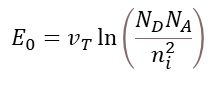
P-N Junction Formula
The formula used in the P-N junction depends upon the built-in potential difference created by the electric field is given as:
 Where,
- E0 is the zero bias junction voltage
- VT is the thermal voltage of 26mV at room temperature
- ND and NA are the impurity concentrations
- ni is the intrinsic concentration.
Diode Current Equation
The diode current is given by the following relation:
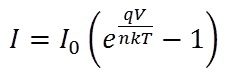
- I is the diode current
- I0 is the dark saturation current,
- q is the charge on the electron,
- V is the voltage applied across the diode,
- η is the (exponential) ideality factor.
- K is the Boltzmann constant which is equal to K = 1.38 x 10⁻²³ J/K
- T is absolute temperature in Kelvin.
V-I Characteristics of pn Junction Diode
The V-I (voltage-current) characteristics of a p-n junction diode shows the relationship between the voltage applied across the diode and the current flowing through it. The V-I curve exhibits distinct behaviour in the forward bias and reverse bias regions.
Normally, voltage is measured along the x-axis, whereas the current is measured along the y-axis.
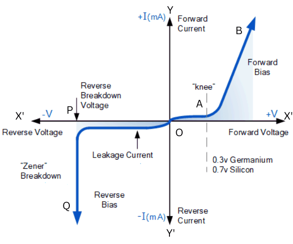
The V-I characteristics of the PN junction diode can be explained in two cases: Forward bias and Reverse bias
When the PN junction diode is in the forward bias, voltage is increased gradually. When the voltage is above the barrier potential 0.7 V, the current starts to increase rapidly.
As shown in the V-I characteristic curve, OA is the non-linear part which shows the starting period where voltage is below 0.7 V and current is very small.
The part AB shows when the voltage is more than the 0.7 V, the curve climbs steeply as the external voltage rises and current increases linearly, yielding a linear curve.
When the PN junction diode is in negative bias, the potential barrier is higher. Due to minority carriers, a small reverse saturation current flows. The current obtained in this state is OP as shown in the graph. When the applied voltage becomes more than the reverse breakdown voltage, a large current will flow due to the avalanche breakdown. In the breakdown region, the V-I curve displays a sharp increase in current, this part is shown as PQ in the graph.
Types of Diodes
There are various types of diodes, each designed for specific applications and operating conditions. Here are some common types of diodes:
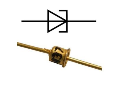
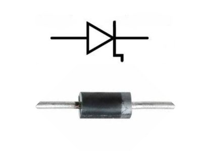
Zener Diode
Zener diode is basically a heavily doped PN junction diode and is used in voltage regulation. It provides a stable reference voltage or to protect circuits from voltage spikes.
They are designed to operate in the reverse breakdown region, maintaining a nearly constant voltage drop across the diode even with varying current.
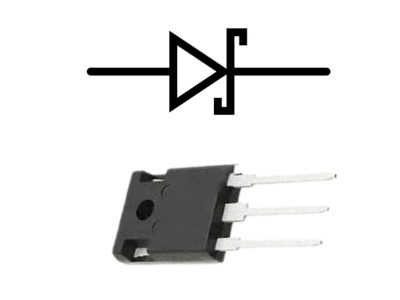
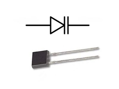
Schottky Diode
Schottky diodes are constructed using a metal-semiconductor junction instead of a traditional P-N junction. This eliminates the depletion region. The benefit of this diode is, it has a lower forward voltage drop and faster switching speed compared to regular diodes. They are commonly used in high-frequency applications, rectifiers, and as clamping diodes in digital circuits.
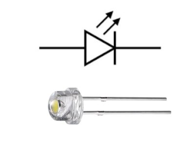
Light-EmittingDiode (LED)
LEDs are semiconductor diodes that emit light in the forward bias configuration. When electrons and holes recombine in the semiconductor material, they emit photons(light). The colour of the light depends on the energy gap of the semiconductor.
They are commonly used as indicators, in displays, and for general lighting purposes. LEDs are available in various colours and can be found in a wide range of electronic devices and lighting applications.
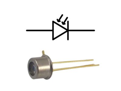
Photodiode
Photodiode is a type of P-N junction diode that converts light energy into electrical current. Photodiodes operate in reverse bias mode. The amount of current generated is proportional to the incident light intensity. When the light (Photon particles) strikes the PN junction, it creates an electron-hole pair resulting in electrical current. To increase its efficiency, a PIN junction diode is used.
They offer several advantages such as high sensitivity, fast response times, and a wide spectral range. They are commonly used in light sensors, optical communication systems, and imaging devices.
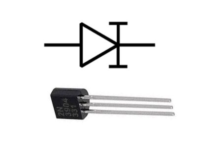
Avalanche Diode
Avalanche diodes are designed to operate in the reverse breakdown region in a controlled manner. They are designed to intentionally exhibit the avalanche effect, where a sudden increase in current occurs when the applied reverse voltage exceeds a specific threshold. Avalanche diode works electrically similar to the Zener diode. However, the doping concentration of a Zener diode is relatively higher as compared to an avalanche diode.
They are often used for applications such as overvoltage protection, high voltage switching, and in microwave circuits.
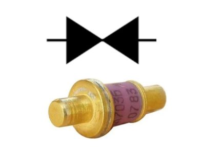
Varactor Diode
Varactor diodes, also known as varicap diodes, are used for voltage-controlled capacitance. By applying a variable reverse bias voltage, the capacitance of the diode can be adjusted. Varactor diodes are commonly used in applications such as voltage-controlled oscillators, frequency modulation, and tuning circuits.
Gunn Diode
A Gunn diode is a three-terminal device that consists of 3 N-type layers. It is made up of semiconductor material like GaAs, InP etc. as these materials exhibit the property of generating microwave oscillations. Gunn diodes exhibit the Gunn effect, which is the phenomenon of negative differential resistance (NDR). This effect is called transferred electron effect and thus the Gunn diodes are also called Transferred Electron Devices.
Gunn diodes are primarily used in high-frequency microwave applications, such as in oscillators and amplifiers.
Tunnel Diode
A Tunnel diode is a heavily doped p-n junction diode in which the current flows because of the tunnelling. Tunneling means a direct flow of electrons across the small depletion region from the n-side conduction band into the p-side valence band. Because of the high level of doping, it can function in both forward bias and reverse bias.
Tunnel diodes are used in specific applications that require fast switching, oscillation generation, and amplification at microwave frequencies.
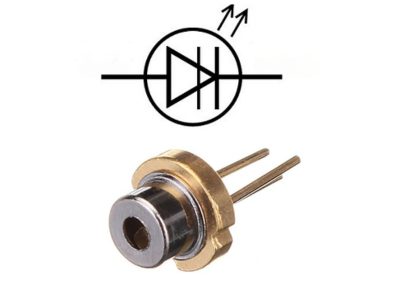
Laser Diode
A laser diode is an optoelectronic device, which converts electrical energy into light energy to produce a high-intensity coherent light in which all the light waves have similar wavelengths. It utilizes the process of stimulated emission to produce a highly focused and intense beam of light.
Laser diodes are extensively used in various devices like barcode readers, security systems, laser printers, fibre optic communications etc.
LASER is an acronym of Light Amplification by Stimulated Emission of Radiation.
PIN Diode
A PIN diode differs from the normal P-N junction diode as it has an extra layer in between the p and the n junctions. In this diode the undoped intrinsic layer of high resistivity is sandwiched between the p-type semiconductor and n-type semiconductor. It is a type of photo detector, used to convert optical signal into an electrical signal.
PIN diodes are used as variable resistors or attenuators in RF circuits, offering precise control over signal levels.
Constant Current Diode
A constant current diode, also called a current limiting diode (CLD), is an electronic device used to regulate or limit current to a maximum value. These devices keep the current flowing through them unaffected even when the voltage changes.
These diodes are used in different circuits like battery chargers, timing & waveform generator circuits. They can also be used as constant current sources mainly for driving LEDs.
Step Recovery Diode
Step recovery diode, also known as charge-storage diode or snap-off diode or memory varactor. It exhibits a unique step recovery characteristic when the bias voltage is abruptly switched from forward to reverse bias. This characteristic enables step recovery diode to generate short-duration, high-frequency pulses. It provides maximum switching speed at LF (low frequency) thus it is also used as a charge-controlled switch.
Step recovery diodes have extensive uses in microwave and RF systems, such as pulse generators, frequency multipliers, and time-domain reflectometers.
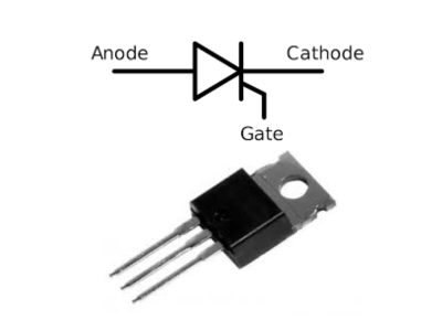
Silicon Controlled Rectifier or Thyristor
Silicon controlled rectifier is a unidirectional current controlling device. It is made of 4 semiconductor layers of alternating P and N type materials. The SCR conducts current in one direction and can be triggered to turn on and off using a control signal.
SCRs are used in power control applications such as power delivered to electric motors, heating systems, lighting control, induction heating, etc.
Applications of Diodes
-
Rectifiers: Diodes are used to change AC current to DC current by removing some part of the signal. Different types of rectifier circuits may be built using diodes.
-
Switching Applications: Fast-switching diodes like Schottky diodes are used in high-speed switching circuits, such as in power supplies, radio-frequency (RF) applications, and digital circuits.
-
Overvoltage Protection: Zener diodes are commonly used as voltage regulators and protect sensitive electronic components from voltage spikes by clamping the voltage at a specific level.
-
Logic Gates: Diodes are key components in the construction of logic gates, which are building blocks for digital circuits and microprocessors. They help control and manipulate the flow of current based on logical operations.
-
Signal Clipping and Clamping: Diodes are employed in circuits for signal clipping and clamping, which involve limiting the amplitude of a signal to a specific range.
-
Voltage Regulation: Diodes, particularly Schottky diodes or germanium diodes, can be used for voltage regulation and stabilization in electronic circuits.
-
Light Emission: Light-emitting diodes (LEDs) are widely used for lighting applications, display panels, indicators, and even in high-resolution screens due to their efficiency, and compact size.
