
The 555 timer is one of the most popular IC and widely used in various electronic circuits due to its versatility, stability and accuracy. It is a monolithic timing circuit that produces highly stable time delays or oscillations with great accuracy.
555 Timer IC was invented by Signetic Corporation in 1970. It is used for timing-related applications such as generating various types of pulses, clock signals, creating precise time delays, etc.
In this comprehensive guide, we will explore the 555 timer, its internal circuit, basic operating principle, and various operating modes.
555 Timer IC Block Diagram
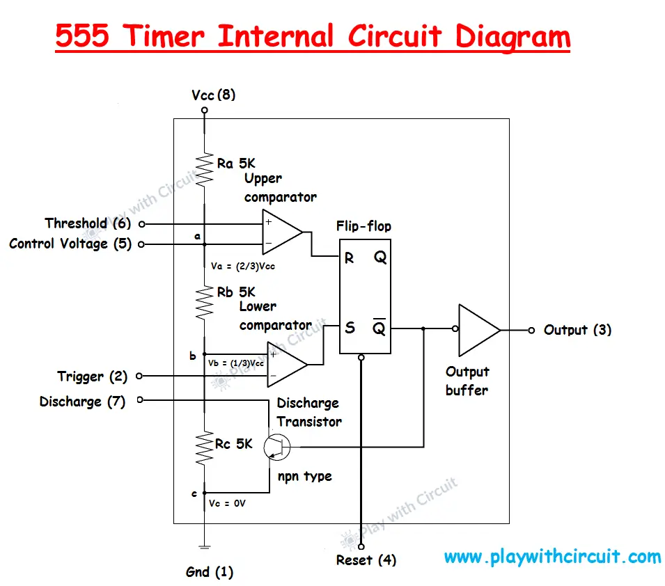
The block diagram of the 555 timer IC is shown in the following figure. It generally come in an 8-pin DIP package. It consists of 2 comparators, a voltage divider circuit made up of three 5KΩ resistors, an SR flip flop, 1 npn transistor, and an output buffer.
555 Timer Working
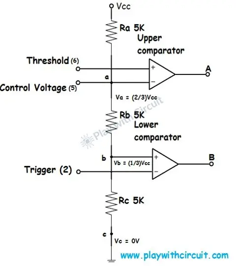
The voltage divider circuit consists of three 5KΩ resistors connected in series between the supply voltage (Vcc) and ground, creating reference voltages at 1/3 and 2/3 of Vcc. These reference voltages are given into the two comparators.
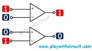
A comparator is a device that compares two analog input voltages at its positive (non-inverting) and negative (inverting) input terminal. If the voltage at the positive terminal is higher than the voltage at the negative terminal, the output of the comparator will be high (1). Conversely, if the voltage at the positive terminal is lower than the voltage at the negative terminal (V-), the output of the comparator will be low (0).
We can control the output of two comparators by the three input pins: Threshold, Trigger, and Control Voltage.
In Upper Comparator or Threshold Comparator, the negative input terminal is connected to a reference voltage 2/3 Vcc and the positive input terminal is connected to the threshold pin (pin 6). When the voltage at the threshold pin exceeds 2/3 Vcc, the comparator outputs a high signal.
In Lower Comparator or Trigger Comparator, the positive input terminal is connected to a reference voltage 1/3 Vcc and the negative input terminal is connected to the trigger pin (pin 2). When the voltage at the trigger pin is less than 1/3 Vcc, the comparator outputs a high signal.
The outputs of the comparators are given as inputs to the SR flip-flop. An SR (Set-Reset) flip-flop is a basic type of memory element that stores a single bit of data. The table below represents the Truth Table of SR flip-flop.
| S | R | Q | Q' |
|---|---|---|---|
| 0 | 0 | Memory | Memory |
| 1 | 0 | 1 | 0 |
| 0 | 1 | 0 | 1 |
| 1 | 1 | Invalid | Invalid |
When S input is high (1), it sets the flip-flop, making the output Q HIGH (1). When R input is HIGH (1), it resets the flip-flop, making the output Q LOW (0). When both S and R inputs are 0, the flip-flop stores the previous value or acts as a memory element. When both S and R inputs are 1 the flip-flop enters in an invalid state. The flip-flop’s output state determines the behavior of the output buffer and the discharge transistor.
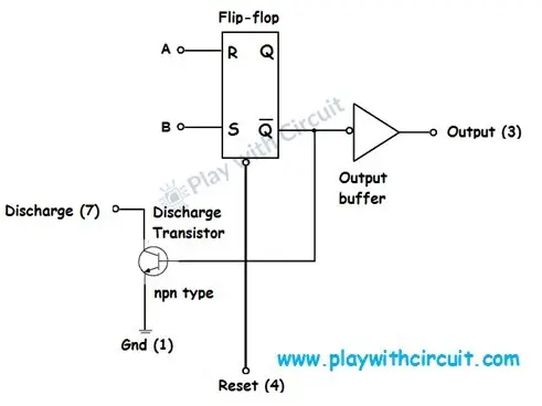
Additionally, the output of the flip-flop is also connected to the base of a discharging transistor. This transistor is used to discharge any externally connected capacitor, ensuring proper circuit functionality. The flip-flops can be reset pin via the external pin called “Reset” that can override two inputs and resets the timer any time.
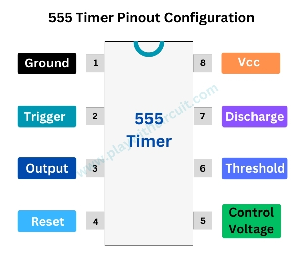
555 Timer Pinout Diagram
555 timer Operating Modes
555 Timer Astable Mode
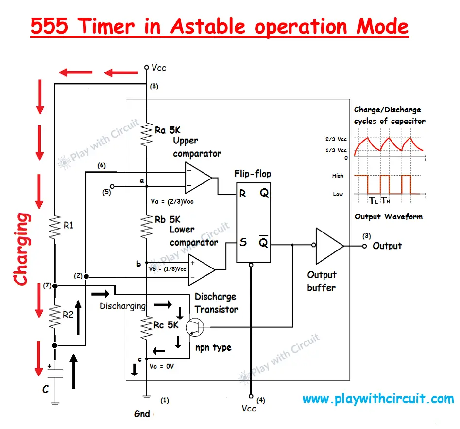
Astable mode as the name suggests, the output of this mode is oscillating between ‘HIGH’ and ‘LOW’ and the frequency of oscillation depends upon an external RC network connected to its pins.
There are two resistors ‘R1’ and ‘R2’ and one capacitor ‘C’. ‘R1’ is connected between pin 8 and pin 7. ‘R2’ is connected between pin 7 and pin 6. Pin 2 and 6 are shorted. Capacitor ‘C’ is connected between pin 6 and the Ground.
Initially when Power is turned ‘ON’, the potential across the capacitor is zero and hence potential at junction ‘b’ is greater than the potential at pin 2 due to which the Output of the lower comparator turns ‘HIGH’ which ‘SETS’ the output of the Flip-flop, i.e., Q is ‘HIGH’ and Q’ is ‘LOW’ which is then fed into output buffer which inverts it and the final output is ‘HIGH’.
Now when the voltage across the capacitor exceeds 1/3 Vcc, it doesn’t have any effect on the lower comparator output. Although the output of the lower comparator turns ‘LOW’, it does not affect the output of S-R flip flop because at this point both inputs S and R is zero hence flip-flip remains at the previous state which was ‘HIGH’.
But as soon as voltage across the capacitor exceeds 2/3 of Vcc the voltage across the positive terminal exceeds voltage across the negative terminal of the upper comparator, which in turn ‘RESETS’ the flip-flop i.e Q turns ‘LOW’ which implies Q’ turns ‘HIGH’ which is fed into Output buffer which inverts it and hence output turns ‘LOW’.
Now what we get from the above operation is when the capacitor charges Output is ‘HIGH’.
Now Q’ which is ‘HIGH’ is also fed to base of npn transitor which in turns provides less resistance (equivalent to zero) for current rather than going through resistance ‘R2’ and Capacitor ‘C’. Hence all the current which previously was flowing through R2 and C now flows through transistor, also the potential across Capacitor ‘C’ starts decreasing because it is also discharging through Discharge transistor.
Now as the capacitor is discharging a point came in this operation when voltage across capacitor turns less than 1/3 Vcc which implies voltage at negative input is less than voltage at positive input, which turns the output of lower comparator ‘HIGH’ and thereby setting the output of flip flop i.e Q is ‘HIGH’ and Q’ is ‘LOW’ , now Q’ is also being fed to base of discharge transistor which turns ‘Off’ thereby discharging stops.
Now what we get from the above operation is when the capacitor discharges output turns ‘LOW’.
Also Q’ is fed to the output buffer and hence voltage at pin 3 turns ‘HIGH’.
This charging and discharging of the capacitor go on and on until power is turned ‘OFF’ or any component failure occurs.
Practical Implementation
Components
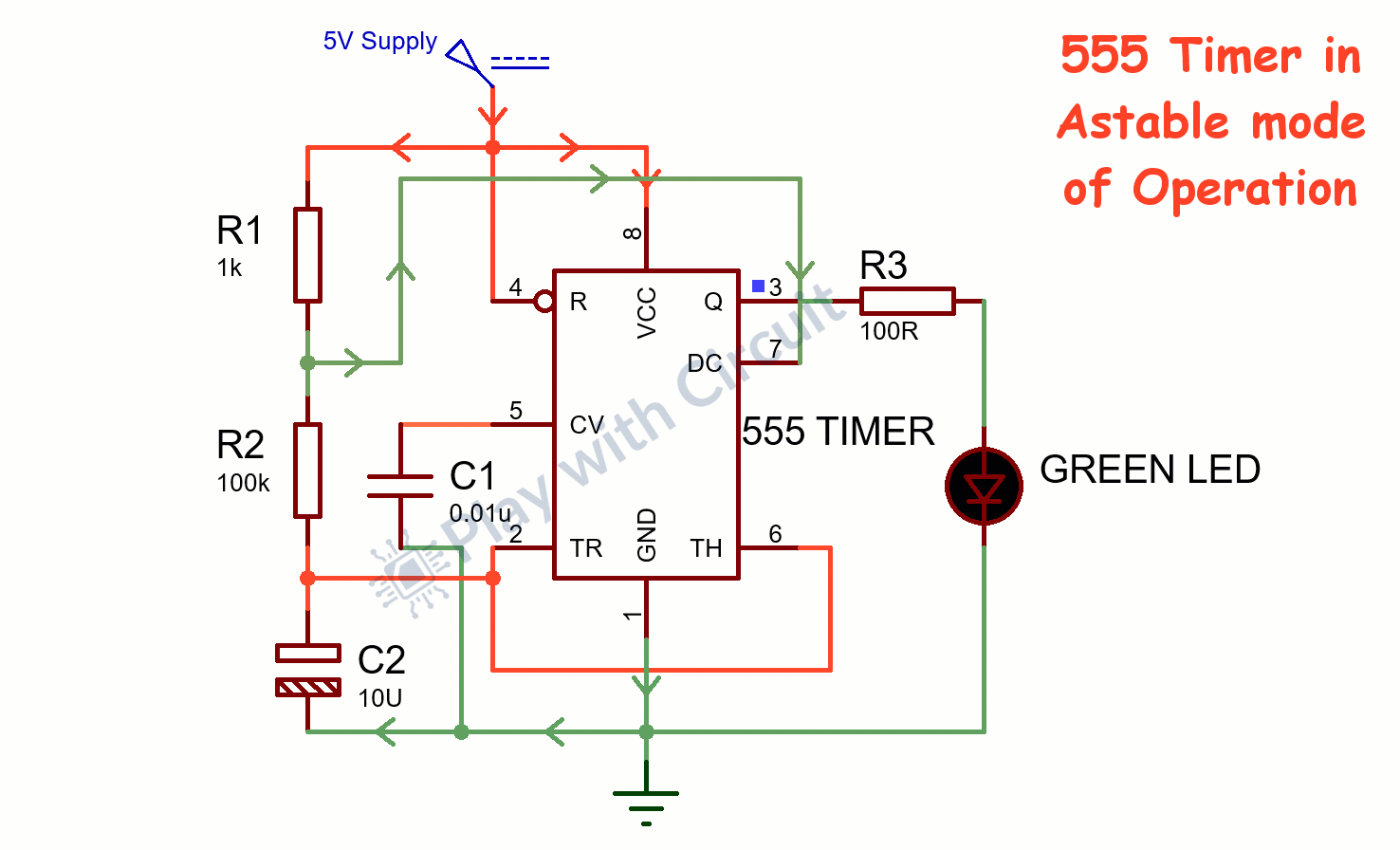
- 555 Timer IC: The main component used to generate the square wave.
- R1 (1kΩ) and R2 (100kΩ): Resistors that set the timing interval for the charging and discharging of the capacitor.
- C1 (0.01µF): A small capacitor connected to pin 5, is used to stabilize the control voltage.
- C2 (10µF): The timing capacitor that charges and discharges to create the square wave.
- R3 (100Ω): Current-limiting resistor for the LED.
- Green LED: The output device that lights up when the output of the 555 timer is HIGH.
 Working
- Power Supply: The circuit is powered by a 5V supply connected to pin 8 (VCC) of the 555 timer IC.
- Charging Phase: When the circuit is powered on, capacitor C2 begins to charge through resistors R1 and R2. As C2 charges, the voltage across it increases. The output (pin 3) of the 555 timer is initially high, causing the LED to light up.
- Threshold and Discharge: Once the voltage across C2 reaches 2/3 of the supply voltage, the 555 timer’s internal comparator triggers the flip-flop, causing the output (pin 3) to go low. The discharge pin (pin 7) is connected to the ground internally, allowing capacitor C2 to discharge through R2.
- Discharge Phase: During the discharge phase, the voltage across C2 decreases. When it falls below 1/3 of the supply voltage, the 555 timer’s internal comparator resets the flip-flop, causing the output to go HIGH again. The discharge pin is disconnected, and the charging process starts again.
- Repetition: This process repeats continuously, creating a square wave output at pin 3. The LED turns ON when the output is high and turns off when the output is low, it is blinking at a rate determined by R1, R2, and C2 values.
Mathematical Derivation
Here we will not go very deep inside the mathematics of charging and discharging curves we just need the output of this astable operation i.e,
Time for which pulse is ‘HIGH’ when current flows through R1, R2, and C (Here ‘C’ represents capacitance of capacitor C2) at charging time i.e.,
T (high) = 0.693(R1+R2)*C
Time for which pulse is ‘LOW’ when current flows through R2 and C at time of discharging i.e.,
T (low) = 0.693(R2)*C
Hence, T(total) = T(high) + T(low)
T = 0.693(R1+2R2)C
F = 1/T = 1.44/((R1+2R2)C)
Duty Cycle = T(high)/T(total)
= 0.693(R1+R2)C/0.693(R1+2R2)C
= (R1+R2)/(R1+2R2)
from the above equation, it seems that the duty cycle is more than 50%.
Let’s say R1 is very less than R2
i.e., if R1 = 1K, then R2 = 100K
Duty Cycle = 101/201 = 0.502 which is approximately equal to 0.5. That’s what we want.
Now this astable multivibrator can be used as a clock source for other circuits which are clock dependent for their operation.
Now for a higher frequency, we need to keep capacitance ‘C’ low for lower frequency, we need to keep ‘C’ high as simple as that.
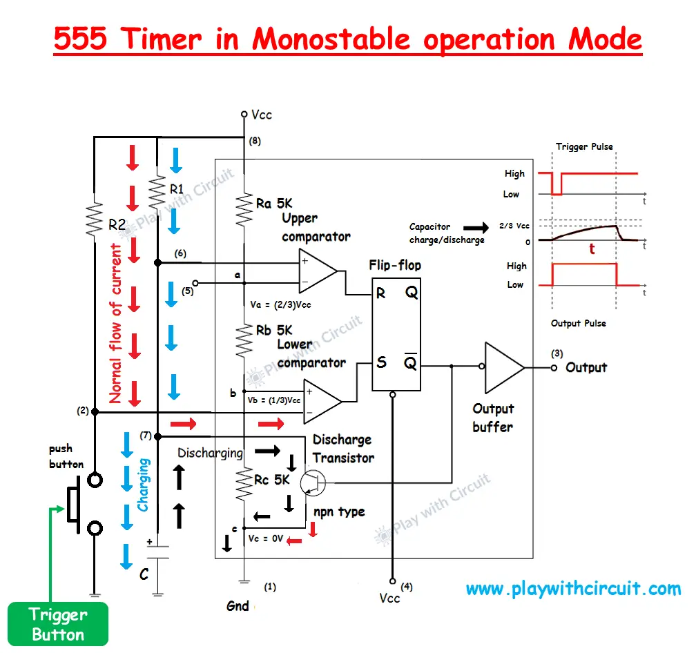
555 Timer Monostable Mode
Practical Implementation
Components
- 555 Timer IC: The core of the circuit, which generates the pulse.
- R1 (10kΩ): Resistor that works with C2 to set the time duration of the output pulse.
- R2 (1kΩ): Resistor connected between the supply voltage and the trigger switch.
- C1 (0.01µF): A capacitor connected to pin 5, used for control voltage stabilization.
- C2 (100µF): Timing capacitor that, along with R2R2R2, determines the pulse width.
- R3 (100Ω): Current-limiting resistor for the LED.
- Green LED: Indicates the output pulse visually.
- Push Button Switch: Provides the trigger input to the circuit.
Working
- Initial State: When the circuit is powered on, the output at pin 3 of the 555 timer is initially LOW, and the LED is OFF.
- Triggering the Circuit: When the push button switch is pressed, it momentarily connects pin 2 (TR, trigger pin) to ground. This causes the voltage at the trigger pin to drop below one-third of the supply voltage, which triggers the 555 timer.
- Generating the Pulse: Once triggered, the 555 timer sets the output at pin 3 to HIGH, turning the Green LED ON. The capacitor C2 starts charging through resistor R2. The voltage across C2 increases exponentially.
- Pulse Duration: The output remains high for a duration determined by the values of R1 and C2. This duration is calculated using the formula: T=1.1×R1×C2. During this time, the LED stays ON, indicating the output pulse.
- End of Pulse: When the voltage across C2 reaches two-thirds of the supply voltage, the 555 timer resets, and the output at pin 3 goes low, turning off the LED. The circuit returns to its initial state, ready to generate another pulse when the trigger button connected at pin 2 is pressed again.
Key Points
- Monostable Mode: The circuit generates a single output pulse each time the trigger is activated.
- Pulse Width Control: The pulse length is controlled by the timing components R1 and C2.
- LED Indicator: The LED provides a visual indication of when the output pulse is active.
This monostable circuit can be used in applications such as timers, delay circuits, and any situation where a precise pulse is required in response to a trigger input.
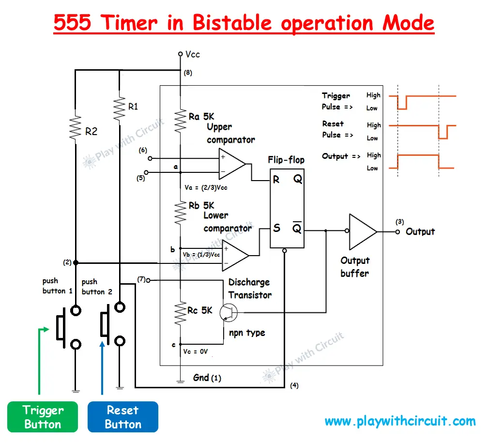
555 Timer Bistable Mode
Practical Implementation
Components
- 555 Timer IC: This is the main component of the circuit.
- Resistors (R1, R2): Two 1kΩ resistors are used.
- Capacitor (C1): A 0.01µF capacitor is connected between pin 5 and GND.
- Resistor (R3): A 100Ω resistor connected in series with an LED.
- LED: A green LED.
- 5V Power Supply: The circuit is powered by a 5V supply.
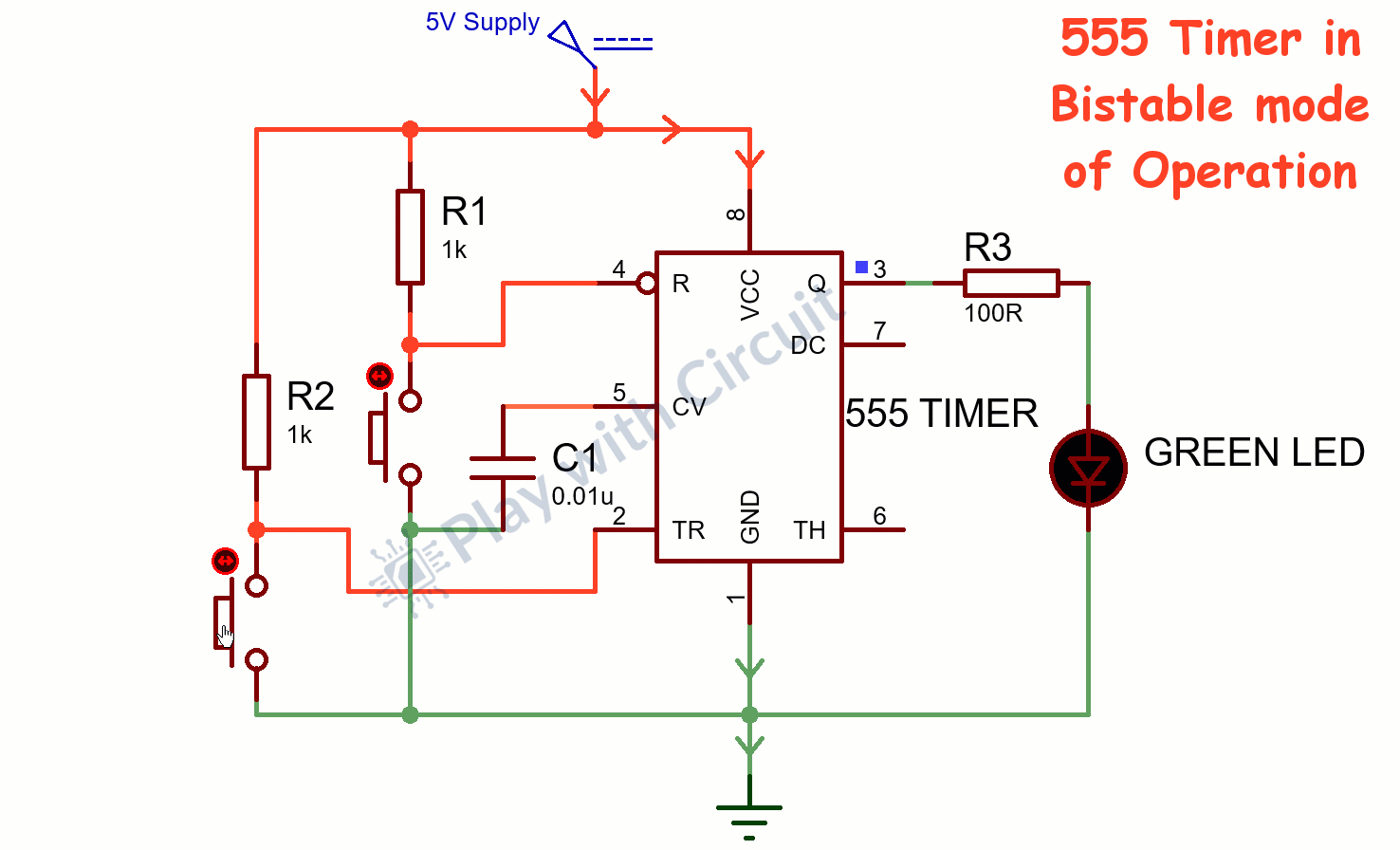
Working
- Initial State: When power is applied to the circuit, the 555 timer operates based on the initial conditions of its trigger and reset inputs.
- Triggering: Pin 2 is used to detect the voltage level. When a low signal is detected at Pin 2, the output at Pin 3 changes state. In bistable mode, once the state is changed, it stays in that state until another trigger signal is detected.
- LED Operation: The green LED connected to Pin 3 will turn ON or OFF depending on the output state of the 555 timer.
- Manual Reset: If Pin 4 (Reset) is pulled LOW, it will reset the 555 timer, turning the output (Pin 3) LOW regardless of the previous state.
FAQ’S
Why is 555 IC called a universal timer?
The 555 timer IC is commonly referred to as the “universal timer” because of its widespread use and versatility in a wide range of electronic applications.
Why is IC 555 called a timer circuit?
The IC 555 is called a because its primary application is to generate accurate time delays or intervals.
What are 555 timers used for?
The 555 timer IC can be used in electronic circuits for various timing and oscillator applications. It is used in various timers, pulse generators, lamp flashers, logic clocks, and oscillators.
