SPI protocol is an indispensable communication interface for high-speed data transfer in electronic systems. SPI is extensively used in interfacing microcontrollers with peripheral devices like sensors, analog-to-digital converters (ADCs), digital-to-analog converters (DACs), shift registers, displays, and static RAM (SRAM).
In this article we will discuss the fundamentals of SPI, how it works and its configurations.
Serial vs Parallel Communication
In electronic devices, data can be transmitted either parallelly or serially. In parallel communication multiple bits are sent simultaneously across separate wires, with each wire carrying a single bit. This allows data to be transmitted quickly, as an entire byte can be transferred at once. However, it requires more wiring, which makes it less practical for longer distances or complex setups.
The following diagram shows the parallel transmission of the letter “S” in binary (01010011):
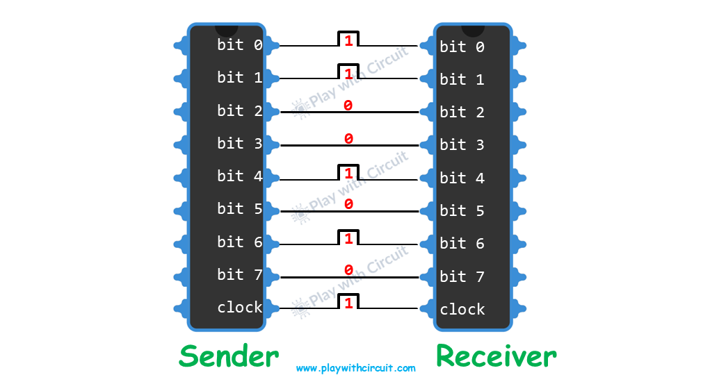
| Bit Position | 7 | 6 | 5 | 4 | 3 | 2 | 1 | 0 |
|---|---|---|---|---|---|---|---|---|
| Binary | 0 | 1 | 0 | 1 | 0 | 0 | 1 | 1 |
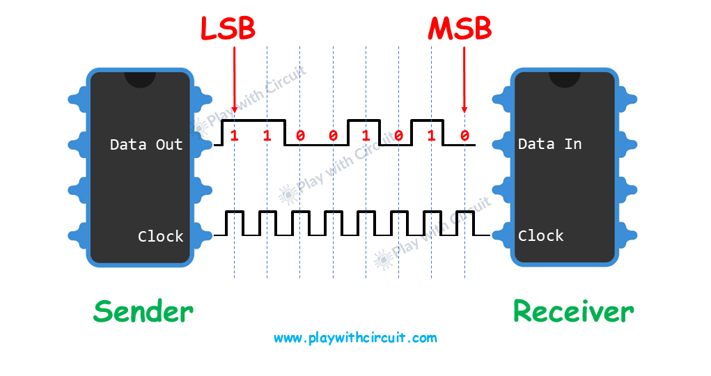
In serial communication data bits are sent one at a time in sequential order through a single wire. This is slower than parallel communication but it simplifies the wiring and is more practical for long-distance transmission or systems with limited I/O pins.
For the same letter S (01010011), each bit would be sent one after the other through a single wire in serial transmission, in MSB first format.
What is SPI Protocol?
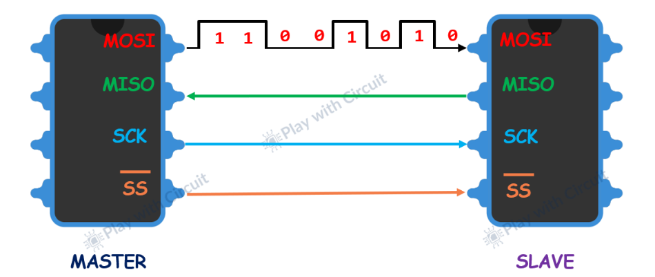
SPI stands for Serial Peripheral Interface. It is a four-wire serial interface used for short-distances and high-speed communication between microcontrollers and peripheral devices, like sensors, displays, ADCs, shift registers and more.
SPI is a synchronous communication protocol. It uses a clock line to synchronize data transmission, making it faster and more reliable for data-intensive applications. The data transmission speed depends on the frequency of the clock generated by the master but is also limited by the clock frequency supported by the slave.
One of the benefits of the SPI protocol is that data can be transferred in a continuous stream without interruption. With I2C and UART protocols data is transmitted in fixed-size packets with start and stop conditions, which interrupts continuous data flow. However, with SPI any number of bits can be sent or received in a continuous data stream.
How SPI Works?
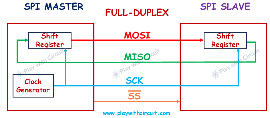
SPI is a full-duplex communication, which means data can be transmitted from both directions at the same time.
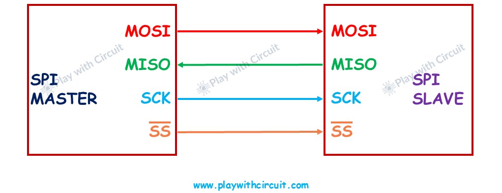
SPI is based on a master-slave architecture where the master is the controlling device which is usually a microcontroller and the slave is usually a peripheral device that takes instructions from the master. The simplest SPI configuration involves a single master device controlling a single slave, but a single master can control multiple slaves.
There are four dedicated communication lines which is required for SPI communication:
- MOSI (Master Output Slave Input): MOSI is a line that sends data from master to slave. Sometimes MOSI is also read as Main Out Subnode In, where Master is referred to as Main and Slave is referred to as Subnode.
- MISO (Master Input Slave Output): MISO is a line that sends data from slave to master. Sometimes MISO is also read as Main In Subnode Out.
- SCK (Serial Clock): SCK is a line for a clock signal generated by the master to synchronize data transfer. Sometimes SCLK is used in place of SCK.
- SS (Slave Select): SS is a line a master uses to select a specific slave for communication. Sometimes CE(Chip Enable) or CS(Chip Select) is used in place of SS. It is an active low signal means the communication will start only when this signal is set to LOW by the master.
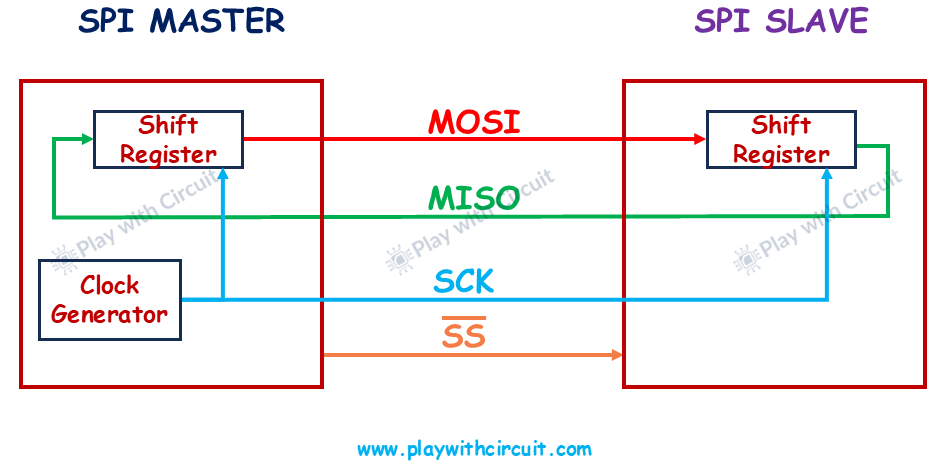
SPI uses the concept of the Shift registers. The master clock generator provides the clock to the shift registers of master and slave.
The shift register is of 8 bits, hence it takes 8 clock pulses to transfer the content of the master’s shift register into the slave’s shift register (Via MOSI line) and at the same time transfer the content of the slave’s shift register into the master’s shift register (Via MISO line).
Serial Peripheral Interface Configurations
SPI configurations are customizable parameters that define how SPI devices communicate with each other. These settings allow developers to adapt SPI communication to specific application requirements. Below is a comprehensive look at key SPI configurations:
Clock Speed (Frequency)
The master generates and initiates the clock signal and the slave receives the data as per clock signal. One bit of data is transferred with each cycle of the clock signal. The speed of data transfer is determined by the frequency of the clock signal. It is expressed in hertz (Hz) and can range from a few kilohertz to several megahertz.
Clock Edges: Rising Edge and Falling Edge
In SPI communication, the clock edges play a crucial role in determining the precise timing for sampling and shifting data during transmission. These edges refer to the transitions of the clock signal between its HIGH and LOW states.
Rising Edge: The rising edge of the clock signal occurs when the signal transitions from a LOW state (0) to a HIGH state (1).
Falling Edge: The falling edge of the clock signal occurs when the signal transitions from a HIGH state (1) to a LOW state (0).

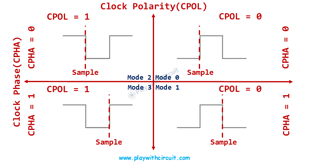
Clock Polarity (CPOL) and Clock Phase (CPHA)
SPI’s clock can be customized using the two properties- clock polarity and clock phase. They work together to control when data bits are sent and received.
Clock Polarity (CPOL)
Clock Polarity (CPOL) defines the idle state of the SPI clock signal (SCK) when no data transmission occurs (i.e., when the communication is idle). It is crucial because it establishes the baseline for timing and synchronization between the master and slave devices.
CPOL = 0: In this case, the clock signal is LOW, when no data is transferred.
CPOL = 1: In this case, the clock signal is HIGH, when no data is transferred.
Clock Phase (CPHA)
Clock Phase (CPHA) determines when data is sampled (read) and when it is shifted (changed) during a clock cycle.
- CPHA = 0: Data is sampled on the leading edge (first edge) of the clock signal and shifted on the trailing edge (second edge).
- CPHA = 1: Data is sampled on the trailing edge (second edge) of the clock signal and shifted on the leading edge (first edge).
The master must select both the CPOL and CPHA bits according to the requirements of the slave device, as both must be synchronized for proper communication.
Data Frame Format and Bit Order
The data frame format defines the structure of each data packet transmitted via SPI. It includes parameters such as the number of bits per frame.
Bit order determines the sequence of data transmission. This configuration specifies whether the Most Significant Bit(MSB) is sent first or the Least Significant Bit(LSB) is sent first.
Both devices in the communication must use the same bit order and data format to ensure accurate data interpretation.
Data Transmission Process in SPI
-
Clock Signal Generation: The master device starts the communication by generating the clock signal (SCK).
-
Slave Selection: The master pulls the target slave’s Slave Select (SS) line LOW.
-
Data Transmission: The master sends data bit-by-bit over the MOSI line. This data is transmitted in sync with the clock signal.
-
Data Reception: Simultaneously, the slave can send data back to the master via the MISO line. SPI’s full-duplex nature allows for simultaneous transmission and reception of data.
-
Clock Edge Synchronization: Data is shifted out and sampled based on the clock edges. The system can be configured to sample data on either the rising or falling edge of the clock signal, depending on the clock polarity (CPOL) and clock phase (CPHA) settings.
-
End of Communication: Once data exchange is complete, the master either deactivates the slave by pulling the SS line HIGH. The clock signal is stopped when the communication concludes.
Communication between one Master and one Slave
Full-Duplex
In full-duplex mode, data flows in both directions simultaneously, allowing both master and slave to transmit and receive data at the same time.
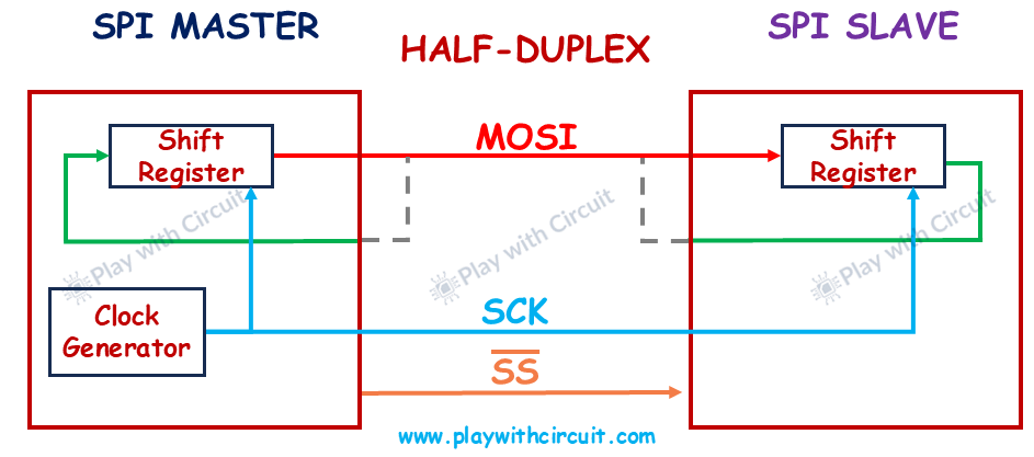
Half-Duplex
In half-duplex mode, data can flow in both directions, but only one direction at a time. Either the master sends data to the slave, or the slave sends data back to the master. It can be achieved either by internally connecting MOSI and MISO lines by configuring SFR’s of SPI bus in microcontroller or by externally connecting the pins using additional active/passive components.
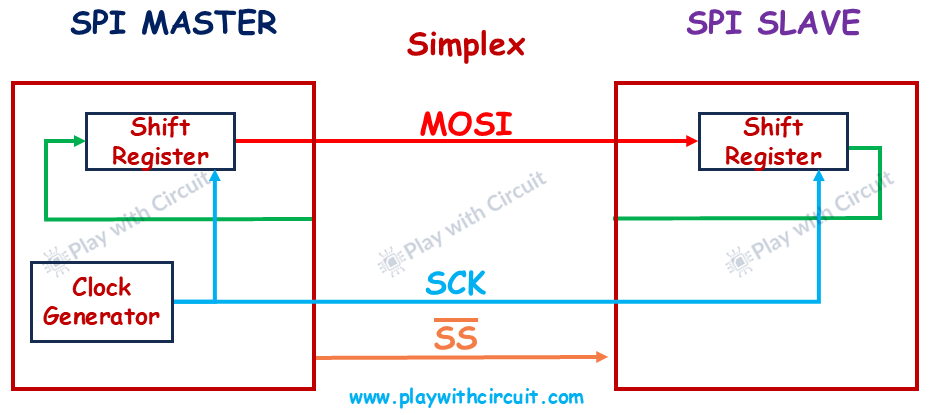
Simplex
In simplex mode, data flows in one direction only— either from the master to the slave or from the slave to the master, but not both simultaneously. In below figure, the direction of data transfer will always be from Master to Slave.
Comparison Table
| Feature | Simplex | Half-Duplex | Full-Duplex |
|---|---|---|---|
| Data Direction | One-way | Two-way (one at a time) | Two-way (simultaneous) |
| Data Flow | Master → Slave or Slave → Master | Bidirectional (not simultaneous) | Bidirectional (simultaneous) |
| MOSI Line | Used only for TX | Shared for TX/RX | Dedicated for TX |
| MISO Line | Not used if MOSI is active | Shared for TX/RX | Dedicated for RX |
| Speed | Fast (single direction) | Medium | Fast (simultaneous) |
| Example | Display module | Temperature sensor | SD card or SPI Flash |
SPI Modes of Operation
SPI supports four modes, each a unique combination of Clock Polarity (CPOL) and Clock Phase (CPHA), which determine how the clock pulse behaves.
These modes define how data is transferred based on the clock polarity and phase settings. Each mode is identified by a number (Mode 0, Mode 1, Mode 2, Mode 3). Below is a summary of the four SPI modes:
| SPI Mode | CPOL | CPHA | Clock Polarity in Idle State | Clock Phase used to Sample and/or Shift (Change) the data |
|---|---|---|---|---|
| 0 | 0 | 0 | Logic low | Data sampled on the rising edge and shifted on the falling edge |
| 1 | 0 | 1 | Logic low | Data sampled on the falling edge and shifted on the rising edge |
| 2 | 1 | 0 | Logic high | Data sampled on the falling edge and shifted on the rising edge |
| 3 | 1 | 1 | Logic high | Data sampled on the rising edge and shifted on the falling edge |
❕Note
The SS line transitions from HIGH to LOW to begin the transmission (start of communication). At the end of the transmission, the SS line transitions from LOW to HIGH, which stops the communication.
Timing Diagrams of SPI modes
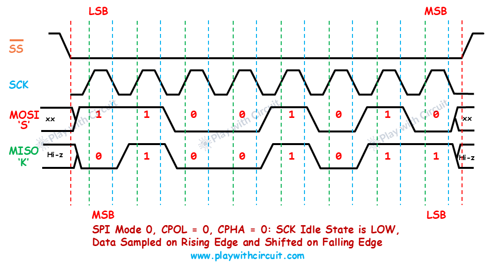
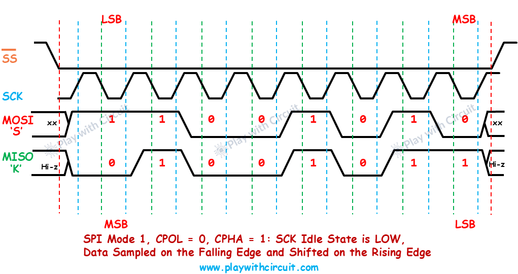
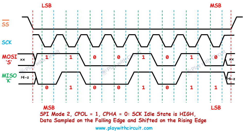
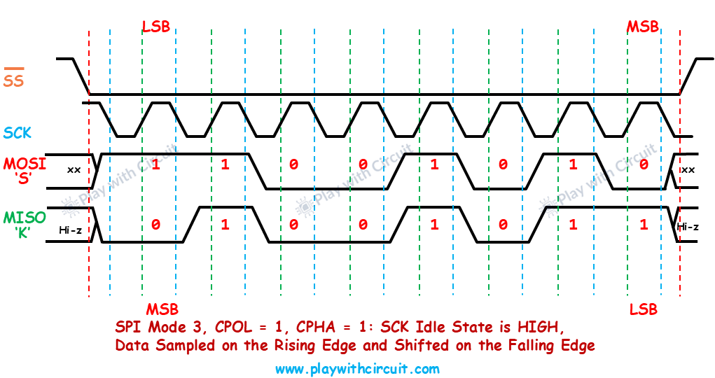
Here the data is shown on the two data lines: MOSI and MISO. Character ‘S’ ( 01010011) is transmitted from MOSI and character ‘K’ ( 01001011) is received on MISO line in MSB first format.
The start and end of data transmission is indicated by the dotted red lines, the sampling edge is indicated in green, and the shifting edge is indicated in blue.
When clock polarity is logic low (0)
SPI Mode 0
Following figure shows the timing diagram for SPI Mode 0. In this mode, the clock phase is configured as 0, so that the data is sampled on the rising edge and shifted on the falling edge of the clock signal. The data should be stable on the MOSI pin before the falling edge on green line.
SPI Mode 1
Following figure shows the timing diagram for SPI Mode 1. In this mode, clock phase is configured as 1, so that the data is sampled on the falling edge and shifted on the rising edge of the clock signal. The data should be stable on the MOSI pin before the falling edge on green line.
When clock polarity is logic high (1)
SPI Mode 2
Following figure shows the timing diagram for SPI Mode 2. In this mode, clock phase is configured as 0, so that data is sampled on the falling edge and shifted on the rising edge of the clock signal. The data should be stable on the MOSI pin before the falling edge on green line.
SPI Mode 3
Following figure shows the timing diagram for SPI Mode 3. In this mode, clock phase is configured as 1, so that data is sampled on the rising edge and shifted on the falling edge of the clock signal. The data should be stable on the MOSI pin before the rising edge on green line.
SPI Configurations based on Slave Connections
Besides the standard configuration, SPI can use a daisy-chain configuration and multiple slave-select configuration. These configurations are based on how slaves are connected with the master.
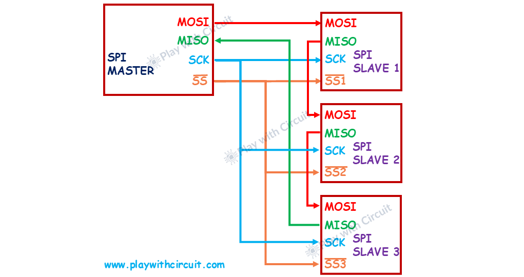
Daisy-Chain Configuration
Daisy-chain configuration simplifies wiring by allowing all slaves to share a common SS line. In this configuration, the MISO of the previous slave connects to the MOSI of the next slave.
Data from the master is transferred sequentially from one slave to the next, with each slave processing its data and passing the remaining bits down the chain.
This configuration significantly reduces the number of SS lines required, conserving GPIO pins on the master device. However, data propagation through the chain increases latency, as the number of clock cycles required grows with the position of the slave in the chain. For instance, in an 8-bit system with three slaves, 24 clock pulses are needed for data to reach the third slave. Additionally, not all SPI devices support daisy-chaining, so compatibility must be verified in the device datasheet. Despite these limitations, daisy-chaining is highly effective for applications requiring sequential data flow, such as individually addressable LED light strings or shift registers.
Multiple Slave-Select Configuration
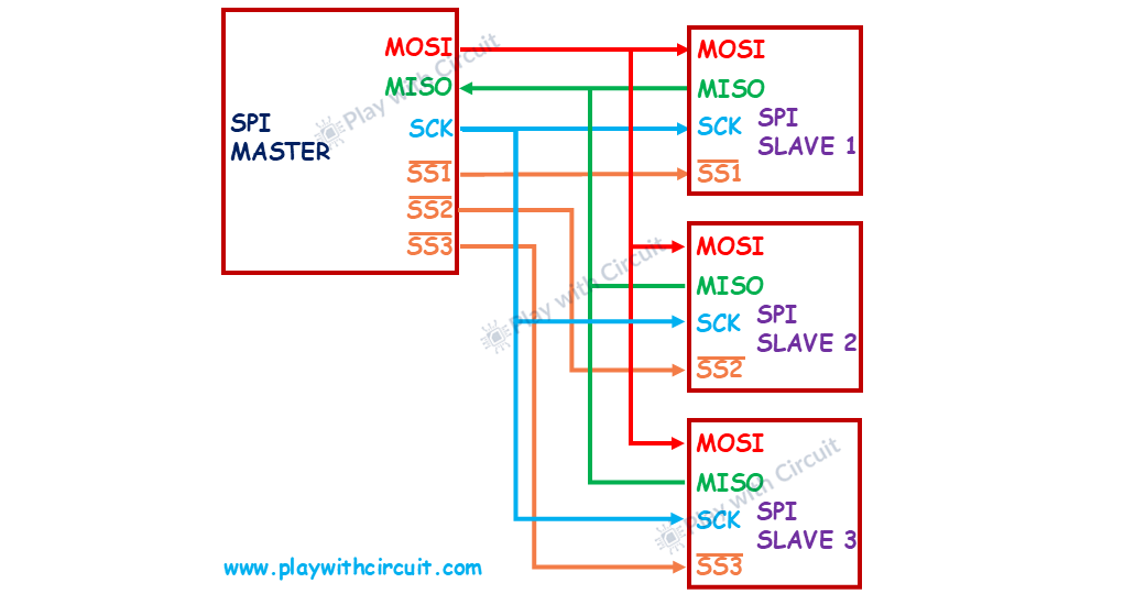
In the multiple-slave-select (MSS) configuration, each slave is assigned a unique slave-select (SS) line from the SPI master. When the master pulls an SS line low, the corresponding slave is activated, enabling data transfer via the shared MOSI and MISO lines.
However, as the number of slaves increases, so does the demand for additional SS lines from the master. This scalability issue can quickly exhaust the GPIO pins available on the master device. To mitigate this limitation, a decoder or demultiplexer, such as the 74HC238, can be employed to generate multiple SS signals using fewer GPIO pins.
Benefits of SPI
- SPI supports high speed data transmission, making it ideal for applications requiring rapid communication, such as displays, memory devices, or real-time data logging.
- Supports Full-Duplex Communication.
- Fewer control bits and no start/stop bits requirement enhance efficiency.
- With four lines, SPI is relatively simple to implement, particularly in comparison to protocols like I²C or UART.
- SPI can interface with multiple slaves using individual slave-select (SS) lines or a daisy-chain configuration
- Unlike I²C, SPI does not require addressing protocols, reducing the communication overhead and improving efficiency.
Limitations of SPI
- SPI doesn’t natively support error-checking.
- SPI is not well-suited for long-distance communication without additional hardware like signal amplifiers.
- For complex systems, managing multiple slaves requires more SS lines or advanced circuitry.
- In SPI, no acknowledgment is sent to confirm the successful receipt of data, unlike I²C which includes an acknowledgment (ACK) signal after each byte of data transmission.

