The 8051 microcontroller is one of the most popular and widely studied microcontrollers in the field of embedded systems. Since its introduction by Intel in 1980, it has become a foundation for learning embedded programming and digital electronics. Although modern microcontrollers such as STM32, ESP32, and AVR offer higher performance and advanced features, the 8051 continues to be extensively used in engineering education because of its simple architecture and ease of programming.
Despite being developed decades ago, the 8051 is used for understanding important embedded system concepts such as memory organization, input/output interfacing, timers, interrupts, serial communication, and embedded programming. Learning the 8051 also provides a solid foundation for working with modern microcontrollers, as many of the core concepts remain the same.
In this comprehensive guide, you’ll learn everything you need to know about the 8051 microcontroller, including its block diagram, architecture, features, memory organization, pin diagram, hardware connections, and applications.
What is the 8051 Microcontroller?
A microcontroller is often referred to as a small computer on a single chip because it integrates all the essential components required to perform a specific task. Unlike a microprocessor, which requires external memory and peripheral devices, the 8051 combines the Central Processing Unit (CPU), program memory (ROM/Flash), data memory (RAM), input/output (I/O) ports, timers/counters, serial communication interface, and interrupt controller on a single integrated circuit (IC). This high level of integration makes the 8051 compact, cost-effective, and suitable for a wide range of embedded applications.
The 8051 is an 8-bit microcontroller, which means its Arithmetic Logic Unit (ALU) and CPU are designed to process 8 bits of data at a time. It also features a 16-bit address bus, allowing it to access up to 64 KB of program memory and 64 KB of external data memory. These capabilities make the 8051 suitable for applications that require reliable real-time control rather than high-performance computing.
8051 Microcontroller Block Diagram
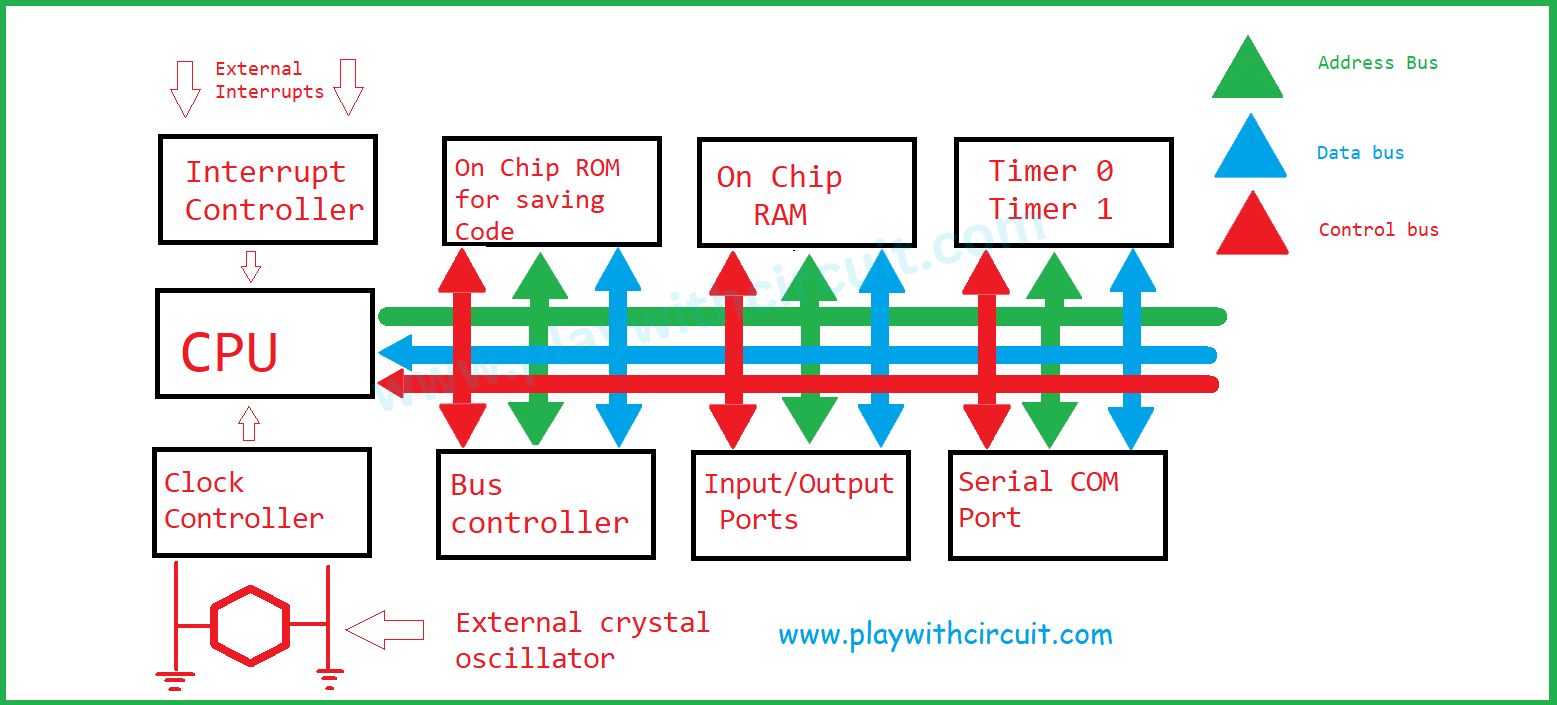
The 8051 microcontroller integrates all the essential hardware components required to build an embedded system on a single chip. These components work together to execute the program, process data, communicate with external devices, and control connected hardware. The functional block diagram of the 8051 microcontroller provides a simplified representation of its internal architecture and illustrates how these functional units are interconnected.
CPU
The CPU acts as the central controller of the 8051. It fetches instructions stored in the program memory, decodes them, executes arithmetic and logical operations, and controls all peripheral devices. During execution, the CPU continuously exchanges information with RAM, timers, I/O ports, and the serial communication unit through the internal system buses.
Memory Organization
The 8051 contains separate memory spaces for storing the application program and temporary data. The Program Memory (ROM) stores the firmware permanently, while the Data Memory (RAM) stores variables, register values, stack data, and intermediate calculation results during program execution.
Timer/Counter Unit
The 8051 microcontroller contains two independent 16-bit Timer/Counters, namely Timer 0 and Timer 1. These timers can be programmed either as timers for generating accurate delays or as counters for counting external events.
Input/Output Ports
The 8051 provides 32 programmable Input/Output (I/O) pins, organized into four 8-bit ports: Port 0 (P0), Port 1 (P1), Port 2 (P2) and Port 3 (P3)
These ports allow the microcontroller to communicate with external hardware such as LEDs, switches, LCDs, keypads, relays, sensors, motors, and many other electronic devices. Each port pin can be configured as either an input or an output through software.
Serial Communication Port (UART)
The 8051 includes one Full-Duplex Universal Asynchronous Receiver/Transmitter (UART), commonly referred to as the Serial Communication Port. This peripheral enables serial communication between the 8051 and other devices such as: Personal computers, other microcontrollers, GSM modules, Bluetooth modules and sensors. Since it supports full-duplex communication, data can be transmitted and received simultaneously.
Interrupt Controller
The Interrupt Controller allows the CPU to respond immediately whenever an important event occurs, instead of continuously checking every peripheral. When an interrupt is generated, the CPU temporarily suspends the current program, executes the corresponding Interrupt Service Routine (ISR), and then resumes normal program execution from where it stopped.
The standard 8051 supports five interrupt sources: External Hardware Interrupt 0 (INT0), Timer 0 Interrupt, External Hardware Interrupt 1 (INT1), Timer 1 Interrupt (TF1) and Serial Port Interrupt (RI/TI). Interrupts improve the responsiveness and efficiency of embedded applications.
Clock Controller
All operations inside the microcontroller must occur in synchronization. This synchronization is provided by the Clock Controller. The clock controller receives the clock signal generated by the external crystal oscillator connected to the XTAL1 and XTAL2 pins and distributes it throughout the microcontroller. Every instruction executed by the CPU depends on this clock signal.
A crystal frequency of 11.0592 MHz is commonly used because it provides accurate timing for serial communication.
External Crystal Oscillator
The 8051 contains an internal oscillator circuit but requires an external crystal oscillator to generate the system clock.
The crystal oscillator is connected between XTAL1 and XTAL2, along with two capacitors, to produce a stable clock signal for the entire microcontroller. The operating speed of the CPU depends on this clock frequency.
Address Bus
The 8051 contains a 16-bit Address Bus, which enables the CPU to address up to 64 KB (2¹⁶ locations) of memory. It can be calculated as:
Since there are 16 bits which can either store ‘1’ or ‘0’. Hence total number of combinations are 2¹⁶ = 65536. And one location can store one byte of data hence 65536 x 1 Byte = 64 x 1024 x 1 Byte = 64 Kilo byte = 64KB.
The address bus carries the memory address from the CPU to the required memory location or peripheral device.
Data Bus
The Data Bus is 8 bits wide, allowing the transfer of one byte of data at a time between the CPU, memory, and peripheral devices. Because the data bus is 8 bits wide, the 8051 is classified as an 8-bit microcontroller.
Control Bus
The Control Bus carries various control signals that coordinate communication between the CPU and other functional blocks. These signals determine whether data should be read from memory, written to memory, or transferred between internal peripherals, ensuring synchronized operation throughout the microcontroller.
8051 Microcontroller Architecture
The 8051 microcontroller architecture defines the internal organization of the microcontroller and explains how different functional units such as the CPU, memory, timers, input/output ports, and communication peripherals work together to execute a program. Unlike the block diagram, which introduces the major hardware blocks individually, the architecture focuses on how these blocks are interconnected and communicate with one another.
Harvard Architecture
The 8051 follows the Harvard Architecture, where the program memory and data memory are physically separate. The CPU fetches instructions from the program memory while simultaneously accessing data from RAM. This separation improves execution speed and allows the microcontroller to process instructions more efficiently.
Register Organization
The CPU uses several internal registers to perform calculations and manage program execution efficiently. These include the Accumulator (A), Register B, Program Counter (PC), Data Pointer (DPTR), Stack Pointer (SP), Program Status Word (PSW), and the General Purpose Registers (R0–R7). These registers enable fast data processing and efficient execution of instructions.
Integrated Peripheral Interface
The 8051’s built-in peripherals such as timers, serial communication port, interrupt controller, and programmable I/O ports communicate internally with the CPU through the Address Bus, Data Bus, and Control Bus.
Program Execution
The program stored in the ROM controls the operation of all hardware blocks inside the microcontroller. During execution, the CPU fetches instructions from the program memory, processes data stored in RAM, interacts with external devices through the I/O ports, uses timers for timing operations, and communicates with other devices through the serial port.
Memory Structure
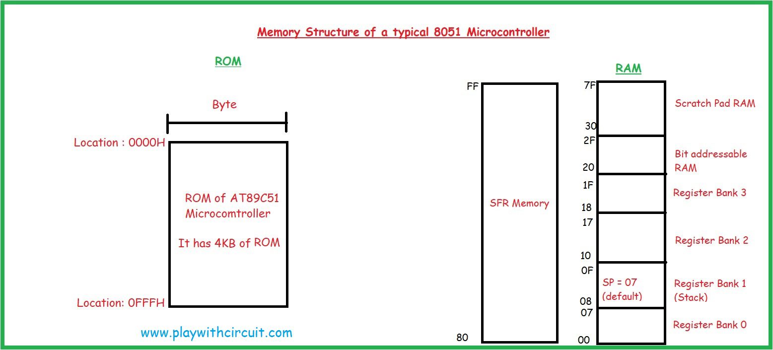
The 8051 microcontroller uses separate memory spaces for storing program instructions and data. The internal memory is divided into Program Memory (ROM), Internal RAM, and Special Function Register (SFR) Memory, each serving a specific purpose.
Program Memory (ROM): The standard 8051 microcontroller provides 4 KB of on-chip Program Memory, ranging from 0000H to 0FFFH. This memory stores the application program that is executed by the CPU after reset.
Internal RAM: The 8051 contains 128 Bytes of Internal RAM (00H–7FH), which is divided into three sections:
-
Register Banks (00H–1FH): Four register banks (Bank 0 to Bank 3), each containing eight general-purpose registers (R0–R7). After reset, Register Bank 0 is selected by default.
-
Bit-Addressable RAM (20H–2FH): A 16-byte memory area where each individual bit can be accessed directly, making it useful for storing flags and status bits.
-
General-Purpose RAM (30H–7FH): Also known as Scratch Pad RAM, this is used to store variables, temporary data, and intermediate results during program execution.
Special Function Register (SFR) Memory: The SFR Memory (80H–FFH) contains registers that control the internal peripherals of the 8051, such as the I/O ports, timers, serial communication, interrupts, and CPU registers. These registers allow the programmer to configure and control the operation of the microcontroller.
8051 Microcontroller Features
- It has 8-bit Central processing unit means CPU can only work on 8-bit data at a time.
- It has 4 Kilo Bytes of programmable space referred to as Read Only Memory (ROM).
- It has 128 Bytes of Random-Access Memory, its used for temporary saving of Data.
- Two independent timers, which can be programmed as timers as well as counters.
- 32 Input output pins which are divided into 4 ports which when act as an output control the external circuit by changing signals both to 5V or 0V and as an input read the input signals within its input range.
- 6 interrupt sources i.e. there are 6 ways to directly interrupt the CPU. When interrupt is occurred then CPU stops running its current code jumps to a special routine executes its code and then restarts its normal running code. All this functioning is controlled by an interrupt controller.
- One serial port which can be used to communicate with other microcontroller and even our personal computers and laptops.
- Address bus is 16-bit unidirectional.
- Data bus is 8-bit bidirectional.
- It has a 16-bit program counter and data pointer.
8051 Microcontroller Pin Diagram
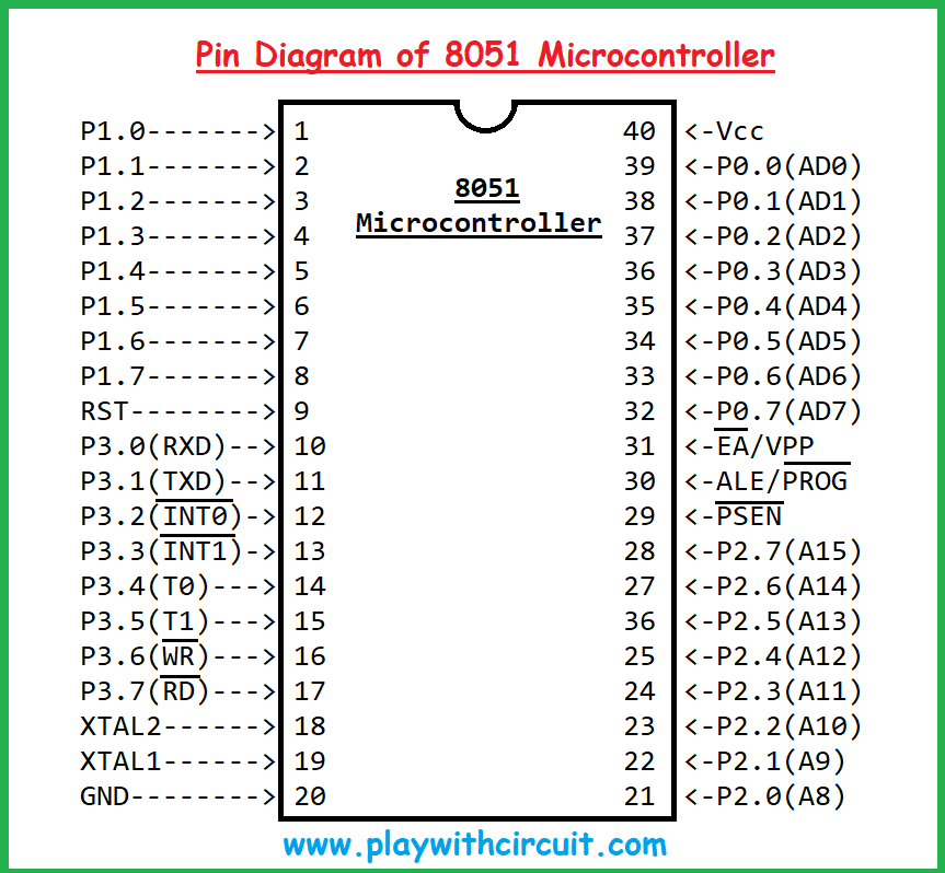
The standard 8051 microcontroller is available in a 40-pin Dual Inline Package (DIP).
Power Supply Pins
The 8051 requires two pins for its power supply.
- VCC (Pin 40): The VCC pin provides the positive supply voltage to the microcontroller. For the standard 8051, this is typically +5 V.
- GND (Pin 20): The GND pin provides the ground reference for the circuit.
Input/Output Ports
One of the most important features of the 8051 is its 32 programmable input/output pins, which are divided into four 8-bit ports:
- Port 0 (P0): Port 0 consists of programmable 8 input/output pins (P0.0–P0.7). Unlike the other ports, Port 0 is an open-drain port, which means it requires external pull-up resistors when used as a general-purpose input/output port. Port 0 also performs a dual function. During external memory access, it acts as the multiplexed lower-order address and data bus (AD0–AD7), allowing the microcontroller to communicate with external memory devices.
- Port 1 (P1): Port 1 consists of 8 programmable input/output pins (P1.0–P1.7) with built-in internal pull-up resistors. Port 1 is dedicated entirely to general-purpose input/output operations. It is commonly used to interface LEDs, push buttons, sensors, and other external peripherals.
- Port 2 (P2): Port 2 also consists of 8 programmable input/output pins (P2.0–P2.7) with internal pull-up resistors. When external memory is not used, Port 2 functions as a normal I/O port. During external memory access, it provides the higher-order address bus (A8–A15) required to access external program or data memory.
- Port 3 (P3): Port 3 consists of 8 programmable input/output pins (P3.0–P3.7). In addition to functioning as a general-purpose I/O port, each pin has a dedicated alternate function that supports communication, timers, interrupts, and external memory operations.
| Pin | Alternate Function | Description |
|---|---|---|
| P3.0 | RXD | Serial data receive pin |
| P3.1 | TXD | Serial data transmit pin |
| P3.2 | INT0 | External Interrupt 0 |
| P3.3 | INT1 | External Interrupt 1 |
| P3.4 | T0 | External input for Timer 0 |
| P3.5 | T1 | External input for Timer 1 |
| P3.6 | WR | Write signal for external data memory |
| P3.7 | RD | Read signal for external data memory |
Oscillator Pins
The 8051 requires an external crystal oscillator to generate the system clock.
XTAL1 (Pin 19): XTAL1 serves as the input to the internal oscillator circuit and is connected to one terminal of the external crystal.
XTAL2 (Pin 18): XTAL2 serves as the output of the internal oscillator circuit and is connected to the other terminal of the crystal.
Reset Pin (RST)
The RST (Reset) pin is an active-high input used to initialize the microcontroller.
External Memory Interface Pins
The 8051 provides three dedicated pins for interfacing with external program memory.
EA (External Access): This pin determines whether the microcontroller executes the program from its internal ROM or an external program memory.
ALE (Address Latch Enable): The ALE pin provides a pulse used to separate the multiplexed address and data signals available on Port 0. It is commonly connected to an external latch when interfacing with external memory.
PSEN (Program Store Enable): The PSEN pin is an active-low output used to enable external program memory during instruction fetch operations. It is connected to the Output Enable (OE) pin of an external ROM or Flash memory device.
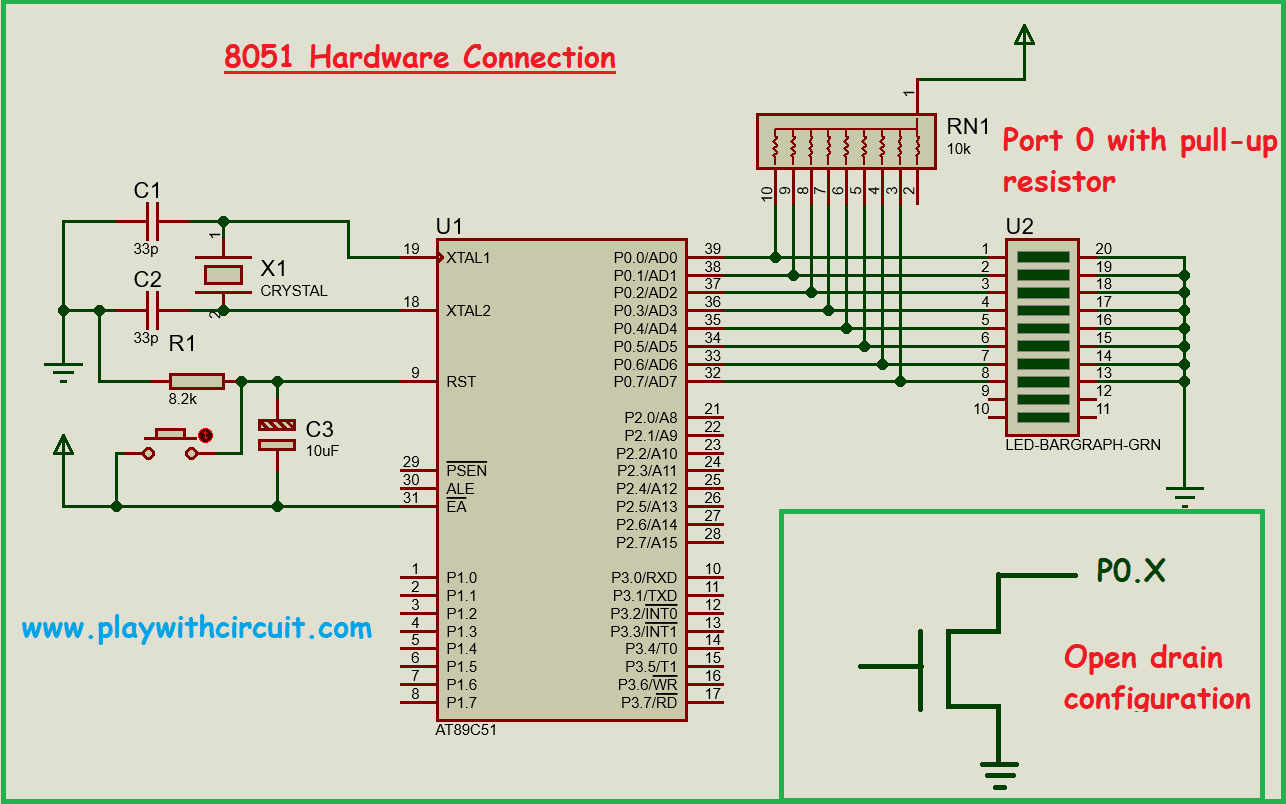
Before the 8051 microcontroller can execute a program, a few essential external components must be connected. These include the power supply, crystal oscillator, reset circuit, and Port 0 pull-up resistors.
Together, these components provide the clock signal, initialize the microcontroller during power-up, supply the required operating voltage, and ensure proper operation of Port 0 when it is used as a general-purpose I/O port.
The following hardware connections represent the minimum circuitry required to operate a typical 8051 microcontroller.
Working of 8051 Microcontroller
The working of the 8051 microcontroller begins as soon as power is applied to the circuit. The external reset circuit initializes the microcontroller, while the crystal oscillator generates the clock signal required for CPU operation. After reset, the CPU starts executing the program stored in the internal program memory from address 0000H.
The complete working of the 8051 can be explained as follows:
Power-On and Reset
When the power supply is applied, the reset circuit generates a high pulse on the RST pin. This initializes the internal registers and prepares the microcontroller for program execution.
Clock Generation
The crystal oscillator connected between XTAL1 and XTAL2 generates the clock signal. This clock synchronizes all operations performed inside the microcontroller.
Instruction Fetch
After reset, the CPU begins fetching program instructions stored in the Program Memory (ROM). The first instruction is fetched from memory location 0000H.
Instruction Decode
The fetched instruction is decoded by the CPU to determine the required operation, such as data transfer, arithmetic calculation, logical operation, or peripheral control.
Instruction Execution
The CPU executes the decoded instruction. During execution, it may: read or write data in RAM, perform arithmetic or logical operations or control timers and counters.
Output Generation
Based on the program, the microcontroller sends output signals to connected devices such as LEDs, LCDs, motors, relays, or sensors.
Continuous Execution
The CPU continuously repeats the Fetch → Decode → Execute cycle until the power supply is removed or the microcontroller is reset.
Advantages of 8051 Microcontroller
- Simple architecture, making it ideal for beginners.
- Integrated CPU, memory, timers, and I/O ports on a single chip.
- Low power consumption and compact design.
- Cost-effective for embedded applications.
- Large community support and extensive documentation.
- Easy to program using Assembly Language and Embedded C.
- Wide availability of development boards and software tools.
Disadvantages of 8051 Microcontroller
- Limited processing power due to its 8-bit architecture.
- Small on-chip RAM and program memory compared to modern microcontrollers.
- Lower operating speed than AVR, PIC, ARM Cortex-M, and ESP32 devices.
- Limited built-in peripherals in the standard 8051.
- Not suitable for graphics, multimedia, or complex IoT applications.
FAQ’S
Why is the 8051 called an 8-bit microcontroller?
The 8051 is called an 8-bit microcontroller because its CPU and Arithmetic Logic Unit (ALU) can process 8 bits of data in a single operation. It also has an 8-bit data bus.
How many pins are there in 8051 microcontroller?
8051 microcontroller has a 40-pin dual in-line package (DIP) configuration. This means it has 40 physical pins that can be connected to external components or devices.
What are the ports 3 pins of 8051?
Port 3 (P3) in the 8051 microcontroller consists of eight pins: P3.0 (RXD) and P3.1 (TXD) for serial communication, P3.2 (INT0) and P3.3 (INT1) for external interrupts, P3.4 (T0) and P3.5 (T1) for external timers/counters, and P3.6 (WR) and P3.7 (RD) for controlling external memory or peripherals. These pins serve various functions such as serial data transfer, interrupt handling, timer input, and interfacing with external devices, providing flexibility and expandability to the microcontroller system.
How much memory does the standard 8051 have?
The original Intel 8051 contains 4 KB of on-chip ROM for program storage and 128 Bytes of internal RAM for temporary data storage.
What is the function of the Program Counter (PC) in the 8051?
The Program Counter (PC) is a 16-bit register that stores the address of the next instruction to be executed by the CPU.
Is the 8051 microcontroller still used today?
Yes. Although modern microcontrollers such as Arduino, AVR, and ESP32 are widely used in new products, the 8051 remains popular in engineering education, legacy industrial systems, and certain commercial embedded applications due to its simplicity and extensive documentation.